SNVSC22B October   2023  – June 2024 LM51772

PRODUCTION DATA  

  1.   1
  2. Features
  3. Applications
  4. Description
  5. Pin Configuration and Functions
  6. Specifications
    1. 5.1 Absolute Maximum Ratings
    2. 5.2 Handling Ratings
    3. 5.3 Recommended Operating Conditions
    4. 5.4 Thermal Information
    5. 5.5 Electrical Characteristics
    6. 5.6 Timing Requirements
    7. 5.7 Typical Characteristics
  7. Parameter Measurement Information
  8. Detailed Description
    1. 7.1 Overview
    2. 7.2 Functional Block Diagram
    3. 7.3 Feature Description
      1. 7.3.1  Buck-Boost Control Scheme
        1. 7.3.1.1 Buck Mode
        2. 7.3.1.2 Boost Mode
        3. 7.3.1.3 Buck-Boost Mode
      2. 7.3.2  Power Save Mode
      3. 7.3.3  Programmable Conduction Mode PCM
      4. 7.3.4  Reference System
        1. 7.3.4.1 VIO LDO and nRST-PIN
      5. 7.3.5  Supply Voltage Selection – VSMART Switch and Selection Logic
      6. 7.3.6  Enable and Undervoltage Lockout
        1. 7.3.6.1 UVLO
        2. 7.3.6.2 VDET Comparator
      7. 7.3.7  Internal VCC Regulators
        1. 7.3.7.1 VCC1 Regulator
        2. 7.3.7.2 VCC2 Regulator
      8. 7.3.8  Error Amplifier and Control
        1. 7.3.8.1 Output Voltage Regulation
        2. 7.3.8.2 Output Voltage Feedback
        3. 7.3.8.3 Voltage Regulation Loop
        4. 7.3.8.4 Dynamic Voltage Scaling
      9. 7.3.9  Output Voltage Discharge
      10. 7.3.10 Peak Current Sensor
      11. 7.3.11 Short Circuit - Hiccup Protection
      12. 7.3.12 Current Monitor/Limiter
        1. 7.3.12.1 Overview
        2. 7.3.12.2 Output Current Limitation
        3. 7.3.12.3 Output Current Monitor
      13. 7.3.13 Oscillator Frequency Selection
      14. 7.3.14 Frequency Synchronization
      15. 7.3.15 Output Voltage Tracking
        1. 7.3.15.1 Analog Voltage Tracking
        2. 7.3.15.2 Digital Voltage Tracking
      16. 7.3.16 Slope Compensation
      17. 7.3.17 Configurable Soft Start
      18. 7.3.18 Drive Pin
      19. 7.3.19 Dual Random Spread Spectrum – DRSS
      20. 7.3.20 Gate Driver
      21. 7.3.21 Cable Drop Compensation (CDC)
      22. 7.3.22 CFG-pin and R2D Interface
      23. 7.3.23 Advanced Monitoring Features
        1. 7.3.23.1  Overview
        2. 7.3.23.2  BUSY
        3. 7.3.23.3  OFF
        4. 7.3.23.4  VOUT
        5. 7.3.23.5  IOUT
        6. 7.3.23.6  INPUT
        7. 7.3.23.7  TEMPERATURE
        8. 7.3.23.8  CML
        9. 7.3.23.9  OTHER
        10. 7.3.23.10 ILIM_OP
        11. 7.3.23.11 nFLT/nINT Pin Output
        12. 7.3.23.12 Status Byte
      24. 7.3.24 Protection Features
        1. 7.3.24.1  Thermal Shutdown (TSD)
        2. 7.3.24.2  Over Current Protection
        3. 7.3.24.3  Output Over Voltage Protection 1 (OVP1)
        4. 7.3.24.4  Output Over Voltage Protection 2 (OVP2)
        5. 7.3.24.5  Input Voltage Protection (IVP)
        6. 7.3.24.6  Input Voltage Regulation (IVR)
        7. 7.3.24.7  Power Good
        8. 7.3.24.8  Boot-Strap Under Voltage Protection
        9. 7.3.24.9  Boot-strap Over Voltage Clamp
        10. 7.3.24.10 CRC - CHECK
    4. 7.4 Device Functional Modes
      1. 7.4.1 Overview
      2. 7.4.2 Logic State Description
    5. 7.5 Programming
      1. 7.5.1 I2C Bus Operation
      2. 7.5.2 Clock Stretching
      3. 7.5.3 Data Transfer Formats
      4. 7.5.4 Single READ from a Defined Register Address
      5. 7.5.5 Sequential READ Starting from a Defined Register Address
      6. 7.5.6 Single WRITE to a Defined Register Address
      7. 7.5.7 Sequential WRITE Starting at a Defined Register Address
  9. LM51772 Registers
  10. Application and Implementation
    1. 9.1 Application Information
    2. 9.2 Typical Application
      1. 9.2.1 Design Requirements
      2. 9.2.2 Detailed Design Procedure
        1. 9.2.2.1  Custom Design with WEBENCH Tools
        2. 9.2.2.2  Frequency
        3. 9.2.2.3  Feedback Divider
        4. 9.2.2.4  Inductor and Current Sense Resistor Selection
        5. 9.2.2.5  Output Capacitor
        6. 9.2.2.6  Input Capacitor
        7. 9.2.2.7  Slope Compensation
        8. 9.2.2.8  UVLO Divider
        9. 9.2.2.9  Soft-Start Capacitor
        10. 9.2.2.10 MOSFETs QH1 and QL1
        11. 9.2.2.11 MOSFETs QH2 and QL2
        12. 9.2.2.12 Loop Compensation
        13. 9.2.2.13 External Component Selection
      3. 9.2.3 Application Curves
    3. 9.3 Power Supply Recommendations
    4. 9.4 Layout
      1. 9.4.1 Layout Guidelines
        1. 9.4.1.1 Power Stage Layout
        2. 9.4.1.2 Gate Driver Layout
        3. 9.4.1.3 Controller Layout
      2. 9.4.2 Layout Example
    5. 9.5 USB-PD Source with Power Path
    6. 9.6 Parallel (Multiphase) Operation
    7. 9.7 Constant Current LED Driver
    8. 9.8 Wireless Charging Supply
    9. 9.9 Bi-Directional Power Backup
  11. 10Device and Documentation Support
    1. 10.1 Documentation Support
      1. 10.1.1 Related Documentation
    2. 10.2 Receiving Notification of Documentation Updates
    3. 10.3 Support Resources
    4. 10.4 Trademarks
    5. 10.5 Electrostatic Discharge Caution
    6. 10.6 Glossary
  12. 11Revision History
  13. 12Mechanical, Packaging, and Orderable Information

Parameter Measurement Information

Gate Driver Rise Time and Fall Time


LM51772 Timing Diagram Gate Driver tr , tf
Figure 6-1 Timing Diagram Gate Driver tr , tf

Gate Driver Dead (Transition) - Time
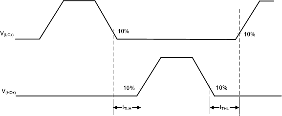

LM51772 Timing Diagram Gate Driver tt
Figure 6-2 Timing Diagram Gate Driver tt