SNVSC22B October 2023 – June 2024 LM51772
PRODUCTION DATA
- 1
- 1 Features
- 2 Applications
- 3 Description
- 4 Pin Configuration and Functions
- 5 Specifications
- 6 Parameter Measurement Information
-
7 Detailed Description
- 7.1 Overview
- 7.2 Functional Block Diagram
- 7.3
Feature Description
- 7.3.1 Buck-Boost Control Scheme
- 7.3.2 Power Save Mode
- 7.3.3 Programmable Conduction Mode PCM
- 7.3.4 Reference System
- 7.3.5 Supply Voltage Selection – VSMART Switch and Selection Logic
- 7.3.6 Enable and Undervoltage Lockout
- 7.3.7 Internal VCC Regulators
- 7.3.8 Error Amplifier and Control
- 7.3.9 Output Voltage Discharge
- 7.3.10 Peak Current Sensor
- 7.3.11 Short Circuit - Hiccup Protection
- 7.3.12 Current Monitor/Limiter
- 7.3.13 Oscillator Frequency Selection
- 7.3.14 Frequency Synchronization
- 7.3.15 Output Voltage Tracking
- 7.3.16 Slope Compensation
- 7.3.17 Configurable Soft Start
- 7.3.18 Drive Pin
- 7.3.19 Dual Random Spread Spectrum – DRSS
- 7.3.20 Gate Driver
- 7.3.21 Cable Drop Compensation (CDC)
- 7.3.22 CFG-pin and R2D Interface
- 7.3.23 Advanced Monitoring Features
- 7.3.24
Protection Features
- 7.3.24.1 Thermal Shutdown (TSD)
- 7.3.24.2 Over Current Protection
- 7.3.24.3 Output Over Voltage Protection 1 (OVP1)
- 7.3.24.4 Output Over Voltage Protection 2 (OVP2)
- 7.3.24.5 Input Voltage Protection (IVP)
- 7.3.24.6 Input Voltage Regulation (IVR)
- 7.3.24.7 Power Good
- 7.3.24.8 Boot-Strap Under Voltage Protection
- 7.3.24.9 Boot-strap Over Voltage Clamp
- 7.3.24.10 CRC - CHECK
- 7.4 Device Functional Modes
- 7.5 Programming
- 8 LM51772 Registers
-
9 Application and Implementation
- 9.1 Application Information
- 9.2
Typical Application
- 9.2.1 Design Requirements
- 9.2.2
Detailed Design Procedure
- 9.2.2.1 Custom Design with WEBENCH Tools
- 9.2.2.2 Frequency
- 9.2.2.3 Feedback Divider
- 9.2.2.4 Inductor and Current Sense Resistor Selection
- 9.2.2.5 Output Capacitor
- 9.2.2.6 Input Capacitor
- 9.2.2.7 Slope Compensation
- 9.2.2.8 UVLO Divider
- 9.2.2.9 Soft-Start Capacitor
- 9.2.2.10 MOSFETs QH1 and QL1
- 9.2.2.11 MOSFETs QH2 and QL2
- 9.2.2.12 Loop Compensation
- 9.2.2.13 External Component Selection
- 9.2.3 Application Curves
- 9.3 Power Supply Recommendations
- 9.4 Layout
- 9.5 USB-PD Source with Power Path
- 9.6 Parallel (Multiphase) Operation
- 9.7 Constant Current LED Driver
- 9.8 Wireless Charging Supply
- 9.9 Bi-Directional Power Backup
- 10Device and Documentation Support
- 11Revision History
- 12Mechanical, Packaging, and Orderable Information
7.3.13 Oscillator Frequency Selection
The LM51772 has a low tolerance internal trimmed oscillator.
It is not recommended to operate in these with the RT pin "open" or short "short" as the frequencies are not accurate. With the RT pin left open, the oscillator frequency is at the min. possible boundary. With the RT pin grounded, the switching frequency is at the maximum possible boundary.
The oscillator frequency can be programmed up or down by connecting a resistor from the RT pin to ground. To calculate the RT resistor for a specific oscillator frequency, use Equation 28.
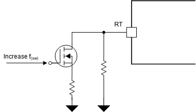
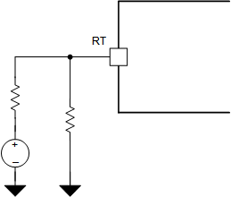
The RT pin is regulated to 0.75V by an internal voltage source when the device is in active mode. Therefore, the switching frequency can be dynamically changed during operation by changing the current flowing through the resistor. Figure 7-24 and Figure 7-25 show two examples for changing the frequency by the switching the resistor value or applying a external voltage source through a resistor. Connecting any additional capacitance directly to the RT pin is not recommended.
 Figure 7-24 Frequency Hopping
Example
 Figure 7-25 Dynamic Frequency Changing
Example