SNVU581B November 2017 – June 2021 TPSM84424 , TPSM84624 , TPSM84824
7 PCB Layout
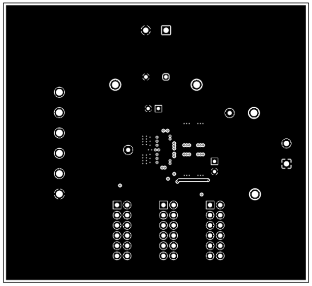
Figure 7-1 through Figure 7-6 show the PCB layers of the TPSM84824EVM, TPSM84624EVM and TPSM84424EVM.
 Figure 7-1 Topside Component Layout (Top View)
 Figure 7-2 Topside Copper (Top View)
 Figure 7-3 Layer 2 Copper (Top View)
 Figure 7-4 Layer 3 Copper (Top View)
 Figure 7-5 Bottom-Side Copper (Top View)
 Figure 7-6 Bottom-Side Component Layout (Bottom View)