SNVU626 November 2020 TPS541620
3 Getting Started
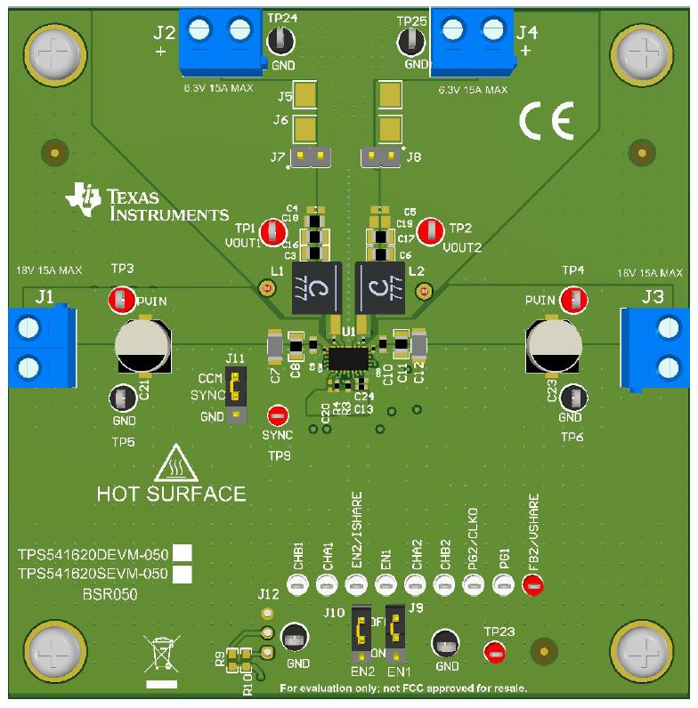
Figure 3-1 illustrates the TPS541620DEVM-050 EVM. The EVM is provided with input/output connectors and test points as shown inTable 4-1 . A power supply capable of supplying 4 A or greater must be connected to J1 and/or J3 through a pair of wires 20AWG or lower . The Vout1 load must be connected to J2 through a pair of wires 20 AWG or lower. The Vout2 load must be connected to J4 through a pair of wires 20 AWG or lower. The maximum load current capability of each output is 6A. Wire lengths should be minimized to reduce losses in the wires. The VIN input voltage can be monitored using TP3 with TP5 as the ground reference or using TP4 with TPS6 as the ground reference. TP1 is used to monitor the output voltage VOUT1 with TP24 as the ground reference. TP2 is used to monitor the output voltage VOUT2 with TP25 as the ground reference.
Make sure jumpers J9 and J10 are set in the ON position which enables both the DC/DC converters on the TPS541620. Jumper J9 enables DC/DC1 and jumper J10 enables DC/DC2 of the TPS541620. Setting the jumpers to the OFF position will disable the DC/DC converter. Apply the input voltage supply of 12V to J1 and/or J3. Connect your oscilloscope or multi-meter probes to the appropriate test points to observe.
 Figure 3-1 TPS541620DEVM-050 PCB
Board
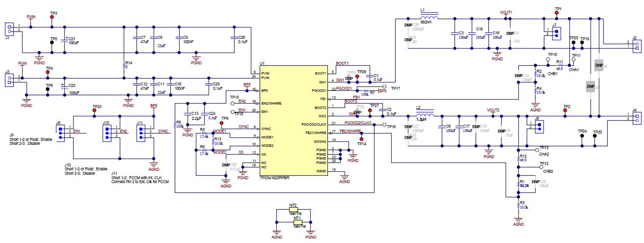
 Figure 3-2 TPS541620DEVM-050
Schematic