SNVU686A November 2020 – May 2021 TPS541620
5 EVM Assembly Drawing and PCB Layout
Figure 5-1 through Figure 5-8 show the design of the EVM printed circuit board.
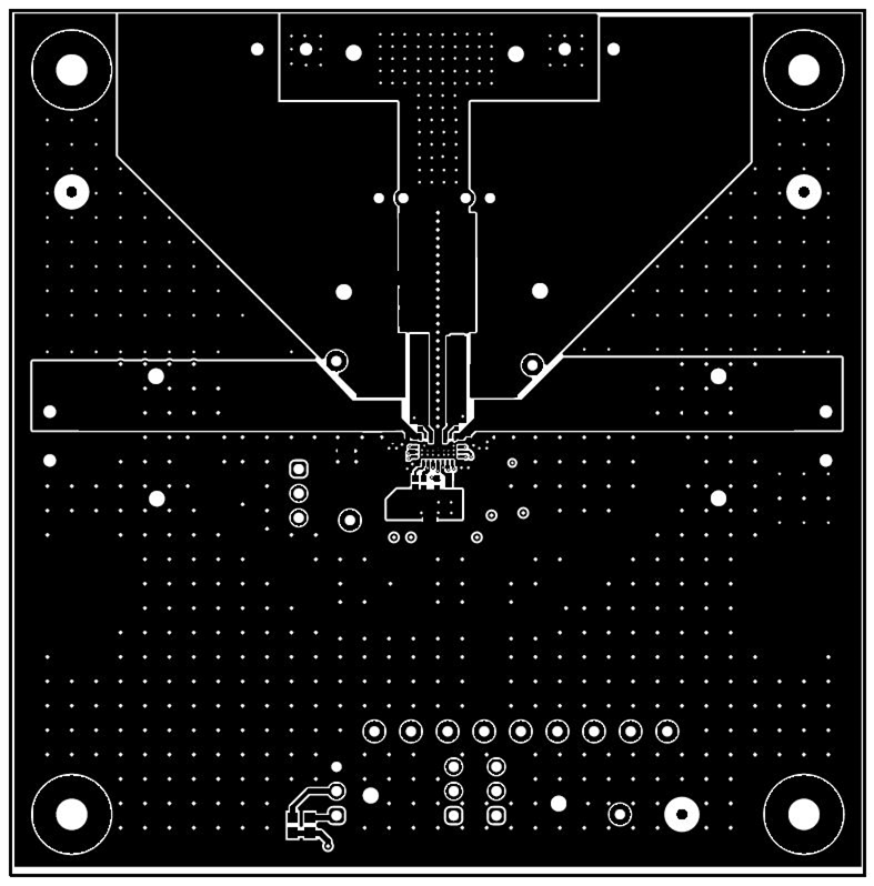 Figure 5-1 Top Layer PCB Drawing
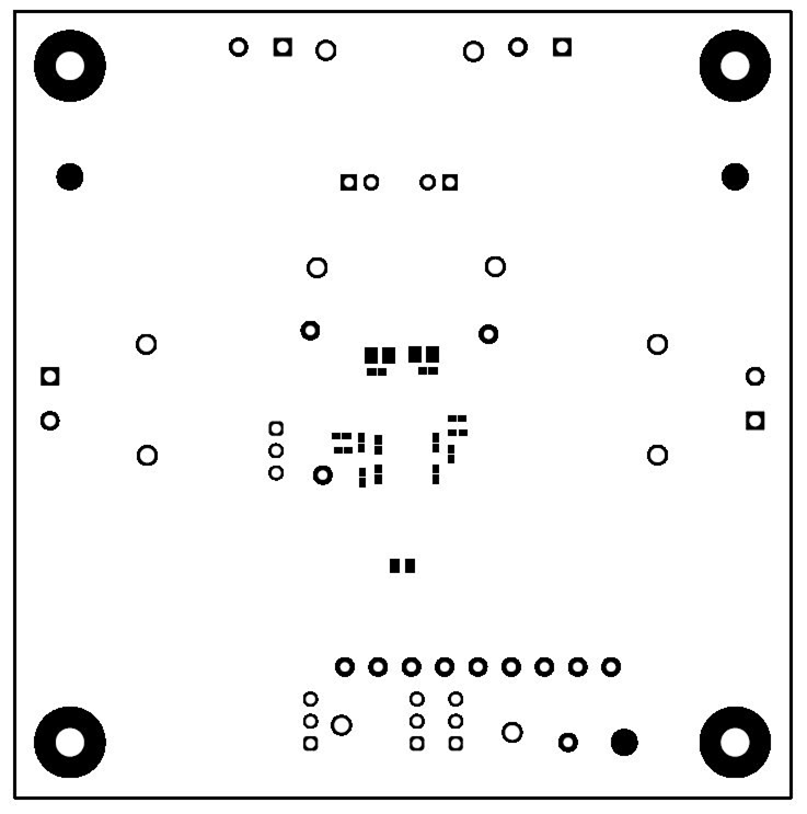 Figure 5-2 Top Layer Solder
Layout
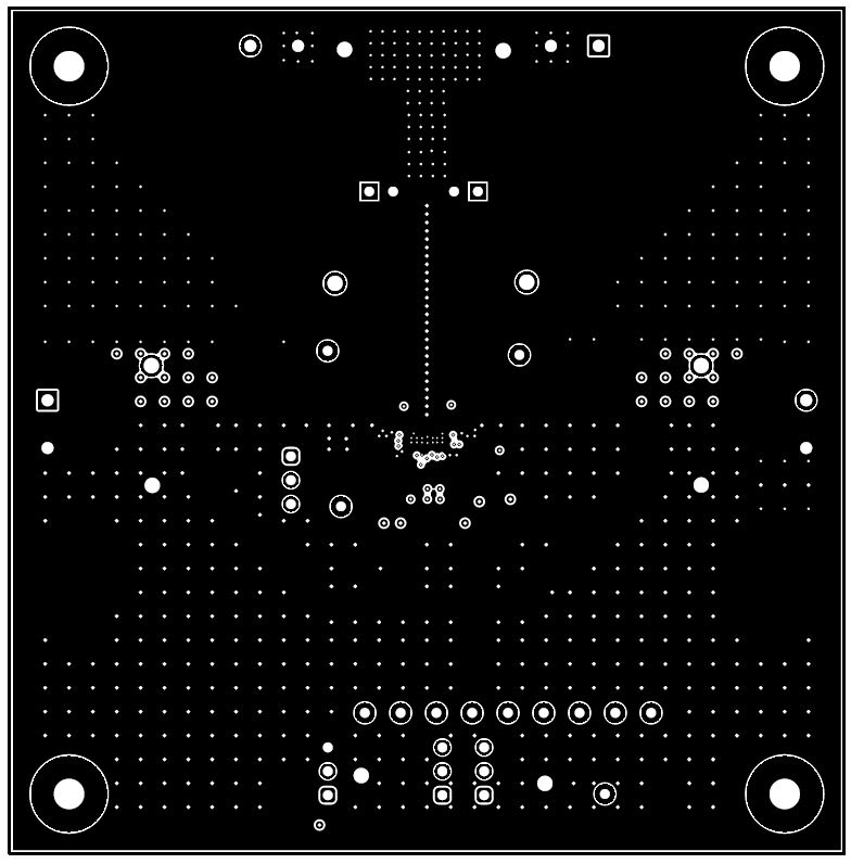 Figure 5-3 Signal Layer 1
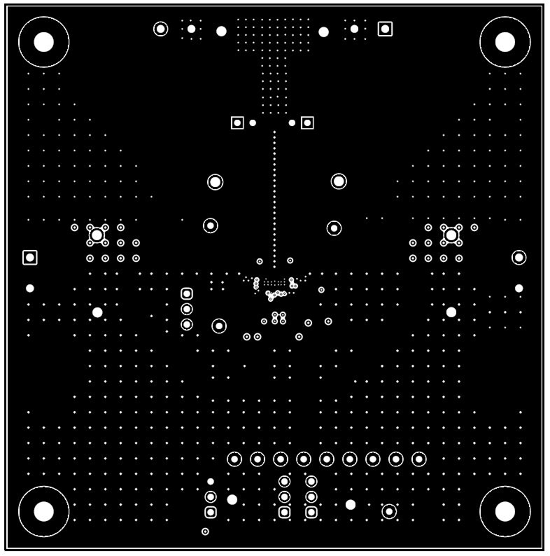 Figure 5-4 Signal Layer 2
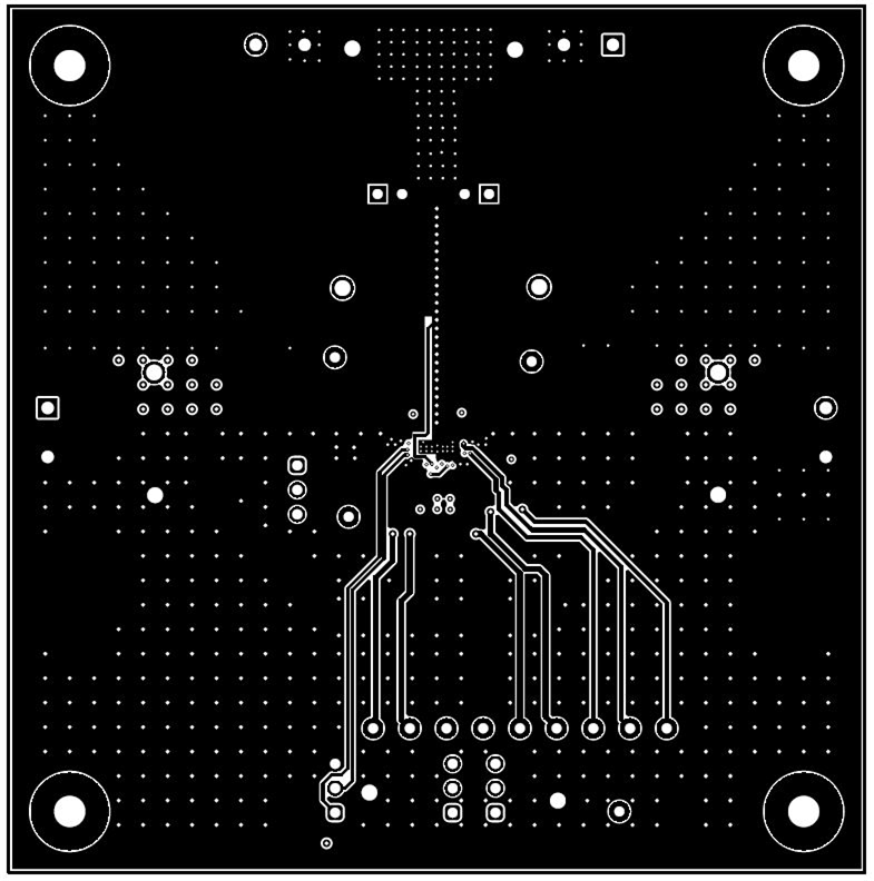 Figure 5-5 Signal Layer 3
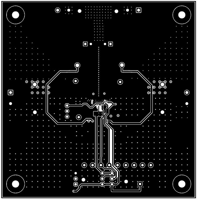 Figure 5-6 Signal Layer 4
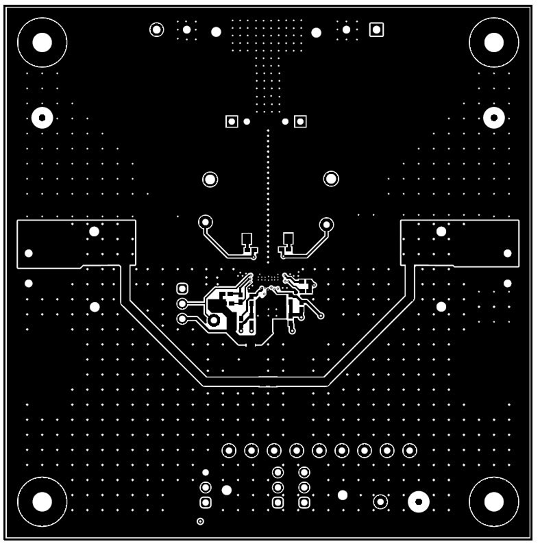 Figure 5-7 Bottom Layer PCB
Layout
 Figure 5-8 Bottom Solder