SNWA014 November 2023 LMH2110
2.3 Simulation Results
In this example for the measurement of reflection coefficient required for VSWR calculation, 50 MHz transmission is assumed which is the lower transmission frequency limit for the power detector LMH2110. The LMH2110 can take a power input from the range -39 dBm to 7 dBm at a frequency of 50 MHz, for which the corresponding output voltage ranges from 0 V to 1.96 V nominally (Section 6.5 of the LMH2110 8-GHz Logarithmic RMS Power Detector with 45-dB Dynamic Range data sheet).
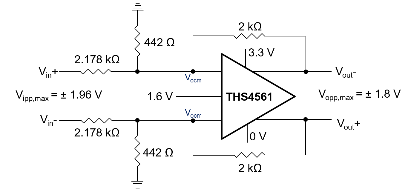
For an input of ±1.96 V (Vipp = 3.92 V), a Vocm of 1.6 V is set externally, the Vcc is set at 3.3 V. For a desired maximum output swing of ±1.8 V (Vopp = 3.6 V), we have derived the values of resistors using circuit loop equations as given in Table 2-1, and the schematic in Figure 2-2 then becomes as shown in Figure 2-3.
 Figure 2-3 THS4561 Test Schematic
| Resistor | Resistance |
|---|---|
| R1 | 2.178 kΩ |
| R2 | 442 Ω |
| R3 | 2 kΩ |
| R4 | 2.178 kΩ |
| R5 | 442 Ω |
| R6 | 2 kΩ |
The recommendation is for the output swing to be always set such that the ADC is not saturated under any circumstance. To have control over the output common mode voltage, the recommendation is to use a voltage reference to set a precise level at the Vocm pin.
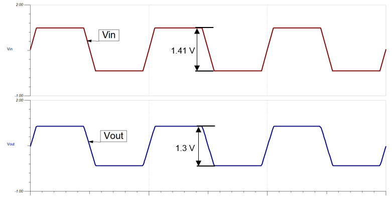
Assuming a signal on the transmission line at 50 MHz with power -10 dBm, and the reflected signal power is measured at -35 dBm. The output voltage of the LMH2110 power detectors correspondingly are 1.237 V and 0.1745 V for forward and reflected power respectively. The input and output graphs are shown in Figure 2-4.
 Figure 2-4 Input and Output Swing of the THS4561 for Given Test Setup
Based on observation, the input and output voltage swing follow a linear relationship for unity gain.