SPRABJ8B September 2022 – November 2023 AM2631 , AM2631-Q1 , AM2632 , AM2632-Q1 , AM2634 , AM2634-Q1 , AM263P4 , AM263P4-Q1
3.1 Crystal and Oscillator Input Options
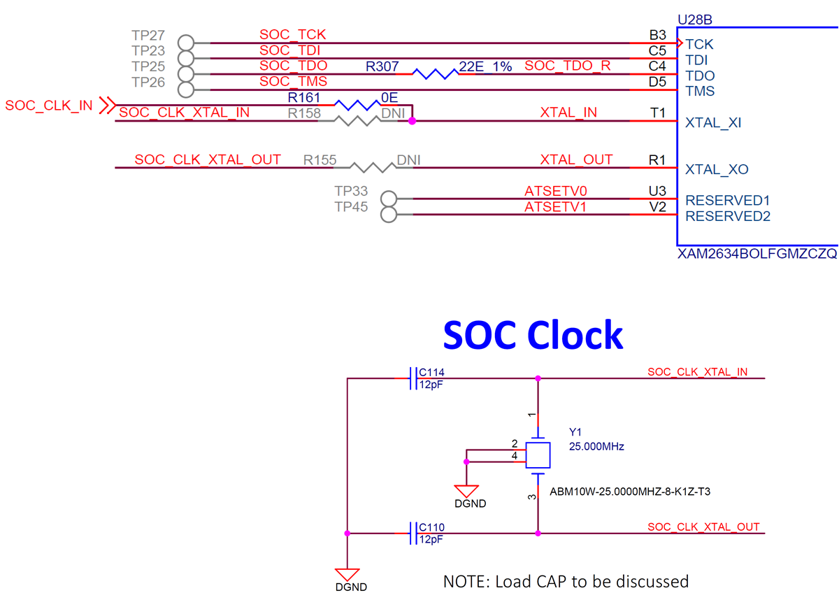
The AM263x and AM263Px XTAL_XI and XTAL_XO (pins T1 and R1) clock input can be sourced from either an attached crystal or a single-ended oscillator output. The attached crystal should be a fundamental mode crystal operating at 25 MHz. If operating from a single-ended oscillator output, the XTAL_XI pin should be connected to the oscillator and the XTAL_XO pin must be left floating, unconnected on the PCB. In oscillator input mode, the XTAL_XI pin can be tied to either a 1.8 V square-wave or sinewave oscillator. For full crystal and oscillator input requirements, see the AM263x Sitara™ Microcontroller Data Sheet or AM263Px Sitara™ Microcontroller Data Sheet.
 Figure 3-1 Excerpt From AM263x Control Card Schematics (for full crystal and oscillator input requirements)
In the case of the AM263x Control Card, an onboard ABM10W-25.0000MHZ-8-K1Z-T3 25 MHz crystal provides crystal mode clocking. Alternatively, an LMK1C1104PWR clock distributor circuit and SN74LV1T34 buffer provide the 1.8 V square-wave clock to the XTAL_XI pin. The LMK1C1104PWR is also used to provide a clock source to the onboard Ethernet PHY as well.
 Figure 3-2 Excerpt From AM263x controlCard Schematics - Oscillator Clock Source and Clock Distributor