SPRACM3E August 2021 – January 2023 F29H850TU , F29H859TU-Q1 , TMS320F280021 , TMS320F280021-Q1 , TMS320F280023 , TMS320F280023-Q1 , TMS320F280023C , TMS320F280025 , TMS320F280025-Q1 , TMS320F280025C , TMS320F280025C-Q1 , TMS320F280033 , TMS320F280034 , TMS320F280034-Q1 , TMS320F280036-Q1 , TMS320F280036C-Q1 , TMS320F280037 , TMS320F280037-Q1 , TMS320F280037C , TMS320F280037C-Q1 , TMS320F280038-Q1 , TMS320F280038C-Q1 , TMS320F280039 , TMS320F280039-Q1 , TMS320F280039C , TMS320F280039C-Q1 , TMS320F280040-Q1 , TMS320F280040C-Q1 , TMS320F280041 , TMS320F280041-Q1 , TMS320F280041C , TMS320F280041C-Q1 , TMS320F280045 , TMS320F280048-Q1 , TMS320F280048C-Q1 , TMS320F280049 , TMS320F280049-Q1 , TMS320F280049C , TMS320F280049C-Q1 , TMS320F28384D , TMS320F28384S , TMS320F28386D , TMS320F28386S , TMS320F28388D , TMS320F28388S , TMS320F28P650DH , TMS320F28P650DK , TMS320F28P650SH , TMS320F28P650SK , TMS320F28P659DH-Q1 , TMS320F28P659DK-Q1 , TMS320F28P659SH-Q1
- Using the Fast Serial Interface (FSI) With Multiple Devices in an Application
- Trademarks
- 1Introduction to the FSI Module
- 2FSI Applications
- 3Handshake Mechanism
- 4Sending and Receiving FSI Data Frames
- 5Daisy-Chain Topology Tests
- 6Star Topology Tests
-
7Event Synchronization Over FSI
- 7.1 Introduction
- 7.2 C2000Ware FSI EPWM Sync Examples
- 7.3 Additional Tips and Usage of FSI Event Sync
- 8References
- 9Revision History
5.1.3 Hardware Control
- Test condition
Device 1 sends data -> Device 2 while receiving the data also passes it back to Device 1 using the hardware channel -> Device 1 receives data back and the CPU verifies it matches the originally sent TX data.
- Test case
Data length of 8 words, two data lines, TXCLK= 30 MHz, with Setting ④ (Table 5-1) enabled.
In this test, while the data packet is being received by the Device 2, it is also simultaneously transmitted out using the pass-through Tx channel. Although, data is verified by the Device 2 for any packet errors, unlike in other modes of transfer, these errors do not prevent the packet from being passed to the Device 1.
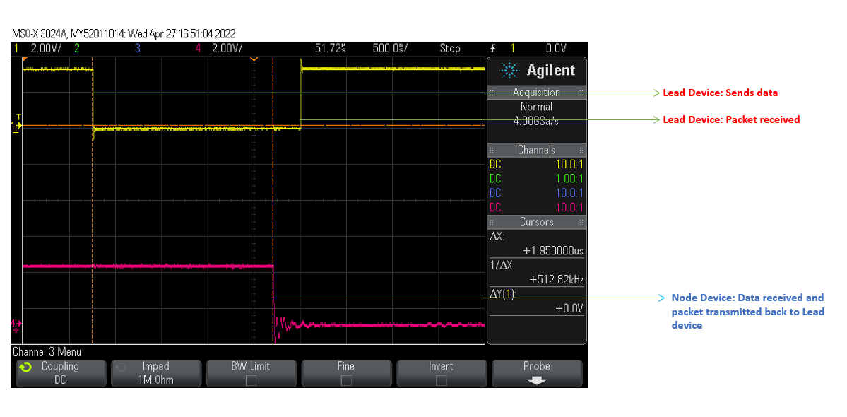
 Figure 5-5 FSI Communication Using HW
Control
Figure 5-5 FSI Communication Using HW
ControlIn the test, GPIOs are toggled within software when specific events occur during the communication and measured using an oscilloscope to obtain the respective timing data. In Figure 5-5, the yellow signal represents the GPIO toggling of Device 1 (Lead device) and the magenta signal represents the GPIO toggling of Device 2 (Node device).As calculated in Equation 1, the theoretical transmission time to send 8 words on two data lines at 30 MHz is 1.6 µs. So, the theoretical interval time between the transmission and reception on lead device is also equal to 1.6 µs (assuming no wire transmission delays) as the hardware control mode exercises the pass-through Rx TDM feature of FSI, which does not have any latencies other than transmission delays. However, the observed value of 1.95 µs from the test includes the time taken to toggle GPIOs, delays introduced by isolators, transceivers, signal propagation delays in the hardware + cables and so forth.
Further test results are given in Table 5-4, for the comparison of using CPU control, DMA control and HW control of FSI. With overhead bits being fixed in the FSI data frame structure, it is beneficial to use a longer data length to maximize the effective data throughput.
| FSITXCLK (MHz) | # of Data Lines | Data Length (16-bit words) | Transmission Time (µs) (1) | Buffer Data Move Time (µs) (1) | Theoretical Transmission Speed (Mbps)(2) | Test Transmission Speed (Mbps) | |
|---|---|---|---|---|---|---|---|
| CPU Control | 50 | 2 | 8 | 1.4 | 4.9 | 175 | 120 |
| 50 | 2 | 16 | 2.1 | 8.3 | 185 | 141 | |
| 50 | 1 | 8 | 2.1 | 4.9 | 100 | 80 | |
| 10 | 1 | 8 | 8.9 | 4.9 | 20 | 18.9 | |
| DMA Control | 50 | 2 | 8 | 1.9 | / | / | |
| 50 | 2 | 16 | 3.0 | / | / | ||
| 50 | 1 | 8 | 2.6 | / | / | ||
| 10 | 1 | 8 | 9.3 | / | / | ||
| HW Control | 30 | 2 |
8 |
1.95 | / | / | |
| 30 | 2 | 16 | 3.05 | / | / | ||
| 12 | 1 | 8 | 7.3 | / | / | ||
There may be cases where FSI communication may need some additional robustness and noise immunity and for that reason a lower clock frequency has also been tested. The FSI protocol is designed to communicate only when there is data exchange. This helps to reduce power and over all EMI in the system. Additionally, lower FSI clock frequencies and half-duplex communication could improve overall system level EMI performance while continuing to provide higher throughput than generic serial ports at the same operating frequencies. Generally, it is best to use a twisted pair or shielded wire per line for board-to-board connections, while on board FSI signal trace lengths should match and have special care taken in the layout to enhance noise immunity.
In the tests performed there are isolation and differential transceiver devices being used on the TMDSFSIADAPEVM boards, which could introduce channel-to-channel skew. In a real world application that utilizes these same or similar devices, and/or varying signal trace lengths, the integrated skew compensation block within the FSI receiver module can be used to manage the skew that may occur between the clock and data signals. For more information on this topic, see Fast Serial Interface (FSI) Skew Compensation.