SPRACN9F May 2023 – August 2024 AM67 , AM67A , AM68 , AM68A , AM69 , AM69A , DRA821U , DRA821U-Q1 , DRA829J , DRA829J-Q1 , DRA829V , DRA829V-Q1 , TDA4AEN-Q1 , TDA4AH-Q1 , TDA4AL-Q1 , TDA4AP-Q1 , TDA4APE-Q1 , TDA4VE-Q1 , TDA4VEN-Q1 , TDA4VH-Q1 , TDA4VL-Q1 , TDA4VM , TDA4VM-Q1 , TDA4VP-Q1 , TDA4VPE-Q1
- 1
- Jacinto7 AM6x/TDA4x/DRA8x LPDDR4 Design Guidelines
- Trademarks
- 1Overview
-
2LPDDR4 Board Design and Layout Guidance
- 2.1 LPDDR4 Introduction
- 2.2 LPDDR4 Device Implementations Supported
- 2.3 LPDDR4 Interface Schematics
- 2.4 Compatible JEDEC LPDDR4 Devices
- 2.5 Placement
- 2.6 LPDDR4 Keepout Region
- 2.7 Net Classes
- 2.8 LPDDR4 Signal Termination
- 2.9 LPDDR4 VREF Routing
- 2.10 LPDDR4 VTT
- 2.11 CK, CMD_ADDR, and CTRL Topologies
- 2.12 Data Group Topologies
- 2.13 CK, CMD_ADDR, and CTRL Routing Specification
- 2.14 Data Group Routing Specification
- 2.15 Channel, Byte, and Bit Swapping
- 3LPDDR4 Board Design Simulations
- 4Revision History
3.5.3.2 Eye Quality
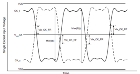
The Vix_DQS ratio and Vix_CK ratio for data write and CA bus simulations are to be verified, at the DRAM pin/BGA. Figure 3-4 from the JEDEC specification explains how to measure the Vix ratio, as well as define the ration requirement(s).
 Figure 3-4 Vix_CK and Vix_DQS Ratio for
Eye Quality
Figure 3-4 Vix_CK and Vix_DQS Ratio for
Eye QualityTable 3-2 Vix_CK and Vix_DQS Ratio for
Eye Quality
| Symbol | Data Rate | Unit | Note | |||||
|---|---|---|---|---|---|---|---|---|
| 1600/1867 | 2133/2400/3200 | 3733/4266 | ||||||
| Vix_CK_ratio | - | 25 | - | 25 | - | 25 | % | (1), (2) |
| Vix_DQS | - | 20 | - | 20 | - | 20 | % | (1), (2) |
(1) Vix_CK_Ratio is defined by the equation: Vix_CK_Ratio =
Vix_CK_FR|Min(f(t))|
(2) Vix_CK_Ratio is defined by the equation: Vix_CK_Ratio =
Vix_CK_RF|Min(f(t))|