SPRACP4A December   2019  – June 2024 AM67 , AM67A , AM68 , AM68A , AM69 , AM69A , DRA821U , DRA821U-Q1 , DRA829J , DRA829J-Q1 , DRA829V , DRA829V-Q1 , TDA4AEN-Q1 , TDA4AH-Q1 , TDA4AL-Q1 , TDA4AP-Q1 , TDA4VE-Q1 , TDA4VEN-Q1 , TDA4VH-Q1 , TDA4VL-Q1 , TDA4VM , TDA4VM-Q1 , TDA4VP-Q1


  1.   1
  2.   Abstract
  3.   Trademarks
  4. 1Introduction
    1. 1.1 Overview
    2. 1.2 Supporting Documentation
  5. 2High-Speed Interface Design Guidance
    1. 2.1  Trace Impedance
    2. 2.2  Trace Lengths
    3. 2.3  Differential Signal Length Matching
    4. 2.4  Signal Reference Planes
    5. 2.5  Differential Signal Spacing
    6. 2.6  Additional Differential Signal Rules
    7. 2.7  Symmetry in the Differential Pairs
    8. 2.8  Connectors and Receptacles
    9. 2.9  Via Discontinuity Mitigation
    10. 2.10 Back-Drill Via Stubs
    11. 2.11 Via Anti-Pad Diameter
    12. 2.12 Equalize Via Count
    13. 2.13 Surface-Mount Device Pad Discontinuity Mitigation
    14. 2.14 Signal Bending
    15. 2.15 ESD and EMI Considerations
    16. 2.16 ESD and EMI Layout Rules
  6. 3Interface-Specific Design Guidance
    1. 3.1 USB Board Design and Layout Guidelines
      1. 3.1.1 USB Interface Schematic
        1. 3.1.1.1 Support Components
      2. 3.1.2 Routing Specifications
    2. 3.2 DisplayPort Board Design and Layout Guidelines
      1. 3.2.1 DP Interface Schematic
        1. 3.2.1.1 Support Components
      2. 3.2.2 Routing Specifications
    3. 3.3 PCIe Board Design and Layout Guidelines
      1. 3.3.1 PCIe Interface Schematic
        1. 3.3.1.1 Polarity Inversion
        2. 3.3.1.2 Lane Swap
        3. 3.3.1.3 REFCLK Connections
        4. 3.3.1.4 Coupling Capacitors
      2. 3.3.2 Routing Specifications
    4. 3.4 MIPI® D-PHY (CSI2, DSI) Board Design and Layout Guidelines
      1. 3.4.1 CSI-2®, DSI® Interface Schematic
      2. 3.4.2 Routing Specifications
      3. 3.4.3 Frequency-Domain Specification Guidelines
    5. 3.5 UFS Board Design and Layout Guidelines
      1. 3.5.1 UFS Interface Schematic
      2. 3.5.2 Routing Specifications
    6. 3.6 Q/SGMII Board Design and Layout Guidelines
      1. 3.6.1 Q/SGMII Interface Schematic
        1. 3.6.1.1 Coupling Capacitors
      2. 3.6.2 Routing Specifications
  7. 4Board Design Simulations
    1. 4.1 Board Model Extraction
    2. 4.2 Board-Model Validation
    3. 4.3 S-Parameter Inspection
    4. 4.4 Time Domain Reflectometry (TDR) Analysis
    5. 4.5 Simulation Integrity Analysis
      1. 4.5.1 Simulator Settings and Model Usage
      2. 4.5.2 Simulation Parameters
      3. 4.5.3 Simulation Methodology
    6. 4.6 Reviewing Simulation Results
  8. 5References
  9. 6Revision History

PCIe Interface Schematic

The PCIe interface schematics vary, depending on the number of lanes implemented and where the reference clock is generated internally or externally. General connectivity is straightforward and consistent between implementations. Figure 3-7 illustrates a single lane, common RefClk Rx clock architecture with device generating the RefClk (output mode).
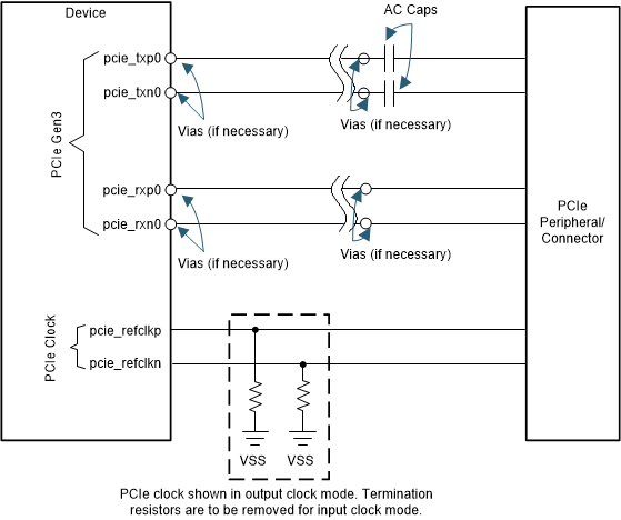
 PCIe Interface High Level SchematicFigure 3-7 PCIe Interface High Level Schematic
Note:

AC coupling capacitors are not shown on the receive data pairs as these capacitors are typically located on the transmit end of the PCIe differential pair.