SPRACP4A December 2019 – June 2024 AM67 , AM67A , AM68 , AM68A , AM69 , AM69A , DRA821U , DRA821U-Q1 , DRA829J , DRA829J-Q1 , DRA829V , DRA829V-Q1 , TDA4AEN-Q1 , TDA4AH-Q1 , TDA4AL-Q1 , TDA4AP-Q1 , TDA4VE-Q1 , TDA4VEN-Q1 , TDA4VH-Q1 , TDA4VL-Q1 , TDA4VM , TDA4VM-Q1 , TDA4VP-Q1
- 1
- Abstract
- Trademarks
- 1Introduction
-
2High-Speed Interface Design Guidance
- 2.1 Trace Impedance
- 2.2 Trace Lengths
- 2.3 Differential Signal Length Matching
- 2.4 Signal Reference Planes
- 2.5 Differential Signal Spacing
- 2.6 Additional Differential Signal Rules
- 2.7 Symmetry in the Differential Pairs
- 2.8 Connectors and Receptacles
- 2.9 Via Discontinuity Mitigation
- 2.10 Back-Drill Via Stubs
- 2.11 Via Anti-Pad Diameter
- 2.12 Equalize Via Count
- 2.13 Surface-Mount Device Pad Discontinuity Mitigation
- 2.14 Signal Bending
- 2.15 ESD and EMI Considerations
- 2.16 ESD and EMI Layout Rules
- 3Interface-Specific Design Guidance
- 4Board Design Simulations
- 5References
- 6Revision History
2.13 Surface-Mount Device Pad Discontinuity Mitigation
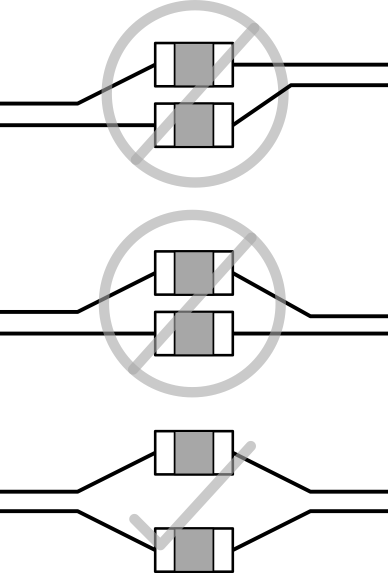
Avoid including surface-mount devices (SMDs) on high-speed signal traces because these devices introduce discontinuities that can negatively affect signal quality. When SMDs are required on the signal traces (for example, the USB SuperSpeed transmit AC coupling capacitors) the maximum permitted component size is 0603. TI strongly recommends using 0402 or smaller. Place these components symmetrically during the layout process to provide the best possible signal quality and to minimize reflection. For examples of correct and incorrect AC coupling capacitor placement, see Figure 2-14.
 Figure 2-14 AC-Coupling Placement
To minimize the discontinuities associated with the placement of these components on the differential signal traces, TI recommends voiding the SMD mounting pads of the reference plane by 100%. Make sure this void is at least two PCB layers deep. For an example of a reference plane voiding of surface mount devices, see Figure 2-15.
 Figure 2-15 Reference Plane Voiding of Surface-Mount Devices