SPRACP4A December   2019  – June 2024 AM67 , AM67A , AM68 , AM68A , AM69 , AM69A , DRA821U , DRA821U-Q1 , DRA829J , DRA829J-Q1 , DRA829V , DRA829V-Q1 , TDA4AEN-Q1 , TDA4AH-Q1 , TDA4AL-Q1 , TDA4AP-Q1 , TDA4VE-Q1 , TDA4VEN-Q1 , TDA4VH-Q1 , TDA4VL-Q1 , TDA4VM , TDA4VM-Q1 , TDA4VP-Q1


  1.   1
  2.   Abstract
  3.   Trademarks
  4. 1Introduction
    1. 1.1 Overview
    2. 1.2 Supporting Documentation
  5. 2High-Speed Interface Design Guidance
    1. 2.1  Trace Impedance
    2. 2.2  Trace Lengths
    3. 2.3  Differential Signal Length Matching
    4. 2.4  Signal Reference Planes
    5. 2.5  Differential Signal Spacing
    6. 2.6  Additional Differential Signal Rules
    7. 2.7  Symmetry in the Differential Pairs
    8. 2.8  Connectors and Receptacles
    9. 2.9  Via Discontinuity Mitigation
    10. 2.10 Back-Drill Via Stubs
    11. 2.11 Via Anti-Pad Diameter
    12. 2.12 Equalize Via Count
    13. 2.13 Surface-Mount Device Pad Discontinuity Mitigation
    14. 2.14 Signal Bending
    15. 2.15 ESD and EMI Considerations
    16. 2.16 ESD and EMI Layout Rules
  6. 3Interface-Specific Design Guidance
    1. 3.1 USB Board Design and Layout Guidelines
      1. 3.1.1 USB Interface Schematic
        1. 3.1.1.1 Support Components
      2. 3.1.2 Routing Specifications
    2. 3.2 DisplayPort Board Design and Layout Guidelines
      1. 3.2.1 DP Interface Schematic
        1. 3.2.1.1 Support Components
      2. 3.2.2 Routing Specifications
    3. 3.3 PCIe Board Design and Layout Guidelines
      1. 3.3.1 PCIe Interface Schematic
        1. 3.3.1.1 Polarity Inversion
        2. 3.3.1.2 Lane Swap
        3. 3.3.1.3 REFCLK Connections
        4. 3.3.1.4 Coupling Capacitors
      2. 3.3.2 Routing Specifications
    4. 3.4 MIPI® D-PHY (CSI2, DSI) Board Design and Layout Guidelines
      1. 3.4.1 CSI-2®, DSI® Interface Schematic
      2. 3.4.2 Routing Specifications
      3. 3.4.3 Frequency-Domain Specification Guidelines
    5. 3.5 UFS Board Design and Layout Guidelines
      1. 3.5.1 UFS Interface Schematic
      2. 3.5.2 Routing Specifications
    6. 3.6 Q/SGMII Board Design and Layout Guidelines
      1. 3.6.1 Q/SGMII Interface Schematic
        1. 3.6.1.1 Coupling Capacitors
      2. 3.6.2 Routing Specifications
  7. 4Board Design Simulations
    1. 4.1 Board Model Extraction
    2. 4.2 Board-Model Validation
    3. 4.3 S-Parameter Inspection
    4. 4.4 Time Domain Reflectometry (TDR) Analysis
    5. 4.5 Simulation Integrity Analysis
      1. 4.5.1 Simulator Settings and Model Usage
      2. 4.5.2 Simulation Parameters
      3. 4.5.3 Simulation Methodology
    6. 4.6 Reviewing Simulation Results
  8. 5References
  9. 6Revision History

Q/SGMII Interface Schematic

The Q/SGMII interface connectivity is straightforward and consistent between implementations. Figure 3-11 illustrates a Q/SGMII system. Ethernet PHY designs include other signals like MDIO that are not included in this guideline. These single ended are slow speed interfaces, and nothing special is required for PCB layout of these signals.
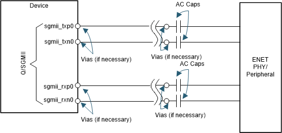
 SGMII Interface High Level SchematicFigure 3-11 SGMII Interface High Level Schematic