SPRACY7 October 2021 TMS320F2800132 , TMS320F2800133 , TMS320F2800135 , TMS320F2800137 , TMS320F2800152-Q1 , TMS320F2800153-Q1 , TMS320F2800154-Q1 , TMS320F2800155 , TMS320F2800155-Q1 , TMS320F2800156-Q1 , TMS320F2800157 , TMS320F2800157-Q1 , TMS320F280033 , TMS320F280034 , TMS320F280034-Q1 , TMS320F280036-Q1 , TMS320F280036C-Q1 , TMS320F280037 , TMS320F280037-Q1 , TMS320F280037C , TMS320F280037C-Q1 , TMS320F280038-Q1 , TMS320F280038C-Q1 , TMS320F280039 , TMS320F280039-Q1 , TMS320F280039C , TMS320F280039C-Q1
3.1 Two Offset Clocks Generated by the SIGGEN0 Module
To generate the same offset clock signals as before using the SIGGEN0 module, the CLKGEN module (which will be clocking SIGGEN0) will be different from the previous example.
The first step is to configure the CLKGEN0 module to generate a clock which will be used by the SIGGEN0 module. To start let's generate CLKGEN0 CLKOUT0 to be EPGCLK divided by 10:
- Setting the CLKDIV0 PRD to be 10 - 1
In the last example with the two offset clocks generated by the CLKGEN0 module, the generated clocks were 100 times slower than EPG clock. So far in this example, the CLKDIV0 has divided EPG clock by a factor of 10. The other divide by 10 will be handled inside the SIGGEN0 module.
The output of the SIGGEN0 module must then be used to drive the EPGOUT0 and EPGOUT1. In this example we will use DATATRANOUT0 and DATATRANOUT2 for EPGOUT0 and EPGOUT1.
To configure the SIGGEN module for generating our offset clock output signals, the following settings are used:
- BIT-BANG mode is NOT used.
- BIT LENGTH of the SIGGEN module is set to 10. This is our DIVIDE 10 for the signal generator, which alongside the CLKDIV0 PRD will generate the EPGCLK/100 output signal frequency. Having a BIT LENGTH of 10, and a CLKDIV PRD of 10 will restrict our output signal offset resolution to be EPGCLK/10.
- Since BIT LENGTH of 10 means that you specify a 10-bit serial stream. For 50% duty cycle of the output signal, the 10 bit serial data is set to "0b0000011111". Each bit in the 10-bit stream will be an (EPGCLK Period)x10 long HIGH/LOW level in the output signal.
- The data to SIGGEN0_DATA0 and SIGGEN0_DATA1 is written by you.
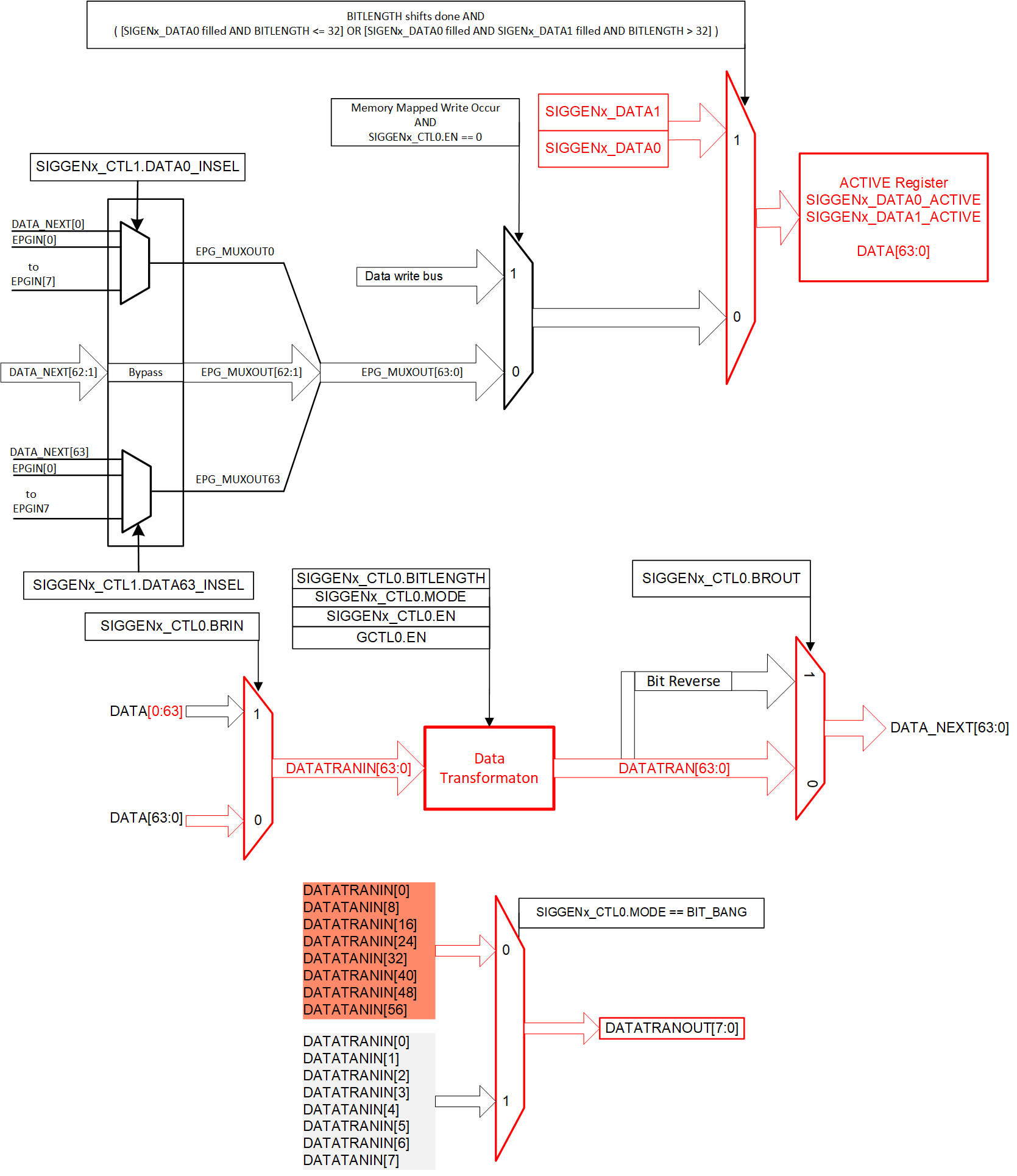
 Figure 3-2 SIGGEN0 Configuration
Generating Two Offset Clocks
Figure 3-2 SIGGEN0 Configuration
Generating Two Offset ClocksSince BIT-BANG mode is not used:
- DATATRANOUT0 ← DATATRANIN0
- DATATRANOUT1 ← DATATRANIN8
- DATATRANOUT2 ← DATATRANIN16
- DATATRANOUT3 ← DATATRANIN24
Currently, DATATRANOUT0 will be used to output DATATRANIN0 for EPGOUT0. For EPGOUT1, DATATRANOUT2 (connected to DATATRANIN16) is used. Since out BIT-LENGTH is set to 10 (10-bit stream), DATATRANOUT1 (connected to DATATRANIN8) is NOT used.
- DATATRANIN0 to DATATRANIN15 used
for the first output (only the first 10 bits are used).DATATRANIN0 → DATATRANOUT0 → EPGOUT0
- DATATRANIN16 to DATATRANIN31 used
for the second output (only the first 10 bits are used).DATATRANIN16 → DATATRANOUT2 → EPGOUT1
Last the SIGGEN module is configure for ROTATE RIGHT REPEAT, to ensure that the data is CONTINUOUSLY generated.
The two 10-bit data streams are concatenated and written to SIGGEN0_DATA0:
- SIGGEN0_DATA0 = (0b0000011111) | ((0b0000011111 << CLOCK_OFFSETS) << 16)
CLOCK_OFFSET can be any value between ZERO and BIT-LENGTH. This will determine the offset between the two output signals. The 16-bit shift, places the second 10-bit stream in SIGGEN0_DATA0 [16:31] which will be tapped at bit 16 by DATATRANOUT2.
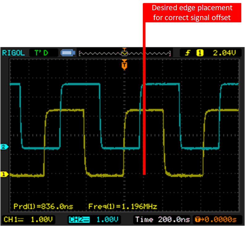
With a 10-bit stream, the second clock output cannot be shifted to exactly match the previous example. If the second serial stream is shifter by 2 bits (CLOCK_OFFSETS = 2), the output will be as shown in Figure 3-3.
 Figure 3-3 Generated Signal Offset -
Shift by 2
Figure 3-3 Generated Signal Offset -
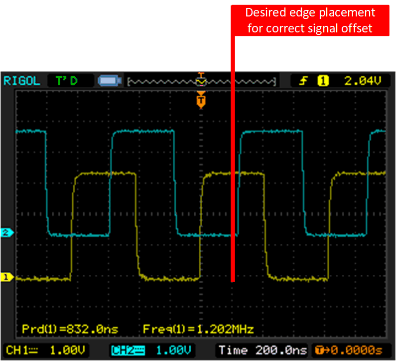
Shift by 2If the second bit stream is shifted by 3 (CLOCK_OFFSET = 3), the output will be as shown in Figure 3-4.
 Figure 3-4 Generated Signal Offset -
Shift by 3
Figure 3-4 Generated Signal Offset -
Shift by 3Since you cannot shift by 2.5 bits, the divider settings must be changed. To perfectly match the signal from the previous example and offset the output signals by 200 ns (F28003x device clocking assumed), the clock divider in CLKDIV0 (CLKGEN0) must be set to 5 and the BIT-LENGTH of the SIGGEN module set to 20. This will ensure the same EPGCLK/100 setting, while allowing a twice higher resolution for the clock offset settings. If the 20-bit serial stream is shifted by 5, the output signals will perfectly match the ones from the previous example.