SPRACY7 October 2021 TMS320F2800132 , TMS320F2800133 , TMS320F2800135 , TMS320F2800137 , TMS320F2800152-Q1 , TMS320F2800153-Q1 , TMS320F2800154-Q1 , TMS320F2800155 , TMS320F2800155-Q1 , TMS320F2800156-Q1 , TMS320F2800157 , TMS320F2800157-Q1 , TMS320F280033 , TMS320F280034 , TMS320F280034-Q1 , TMS320F280036-Q1 , TMS320F280036C-Q1 , TMS320F280037 , TMS320F280037-Q1 , TMS320F280037C , TMS320F280037C-Q1 , TMS320F280038-Q1 , TMS320F280038C-Q1 , TMS320F280039 , TMS320F280039-Q1 , TMS320F280039C , TMS320F280039C-Q1
3.2.5 Shift Right Once - CPOL=1, CPHA=0
In this example, the main difference between ROTATE right once mode and SHIFT right once mode is that after BIT-LENGHT shifts are done in SHIFT RIGHT ONCE mode, the SIGGEN0_DATA0 and SIGGEN0_DATA1 registers are NOT loaded into the active SIGGEN data. Therefore, when SHIFT RIGHT ONCE mode is used, after BIT-LENGTH shifts are done, the IDLE signal level of the data line will be the first bit in the clock stream. The IDLE signal level of the clock line will be the DATA[32] bit that corresponds to SIGGEN0_DATA1[0].
//
// Data
//
#define SIG_GEN_DATA0_0_15    0b1111000011001111U

//
// Clock - Data latched on rising edge
//
#define SIG_GEN_DATA0_16_31   0b1010101010101010U

//
// During idle CLK is HIGH
//
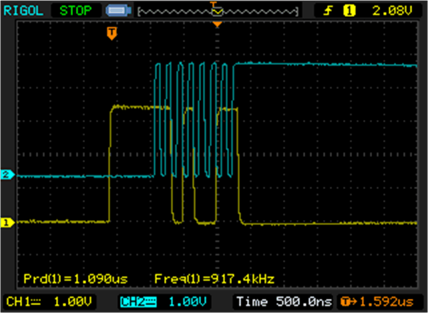
#define SIG_GEN_DATA1_0 0b1When the device PinMux is configured to be driven by Output X-Bar (which is sourced from EPGOUT), while the SIGGEN module is not enable, the signal output on the GPIO is LOW (0). When the SIGGEN module is enabled for the very first time, the generated SPI clock signal will be low until the first "1" in the clock bit stream.
 Figure 3-14 Shift Right Once First Data
and Clock Generation - CPOL=1, CPHA=0
Figure 3-14 Shift Right Once First Data
and Clock Generation - CPOL=1, CPHA=0As shown in Figure 3-14, the SPI clock generated is in the LOW state before the first data and clock pattern is generated. The clock signal IDLE state after the first pattern is generated is HIGH.
In all following transfers, the IDLE state of the clock before and after each pattern generation will always be HIGH.
 Figure 3-15 Shift Right Once All Other
Data and Clock Generation - CPOL=1, CPHA=0
Figure 3-15 Shift Right Once All Other
Data and Clock Generation - CPOL=1, CPHA=0A zoomed in view of the data and clock generated relevant to each other is shown in Figure 3-16.