SPRAD06B March 2022 – November 2024 AM620-Q1 , AM623 , AM625 , AM625-Q1
- 1
- Abstract
- Trademarks
- 1Overview
-
2DDR4 Board Design and Layout Guidance
- 2.1 DDR4 Introduction
- 2.2 DDR4 Device Implementations Supported
- 2.3 DDR4 Interface Schematics
- 2.4 Compatible JEDEC DDR4 Devices
- 2.5 Placement
- 2.6 DDR4 Keepout Region
- 2.7 DBI
- 2.8 VPP
- 2.9 Net Classes
- 2.10 DDR4 Signal Termination
- 2.11 VREF Routing
- 2.12 VTT
- 2.13 POD Interconnect
- 2.14 CK and ADDR_CTRL Topologies and Routing Guidance
- 2.15 Data Group Topologies and Routing Guidance
- 2.16 CK and ADDR_CTRL Routing Specification
- 2.17 Data Group Routing Specification
- 2.18 Bit Swapping
-
3LPDDR4 Board Design and Layout Guidance
- 3.1 LPDDR4 Introduction
- 3.2 LPDDR4 Device Implementations Supported
- 3.3 LPDDR4 Interface Schematics
- 3.4 Compatible JEDEC LPDDR4 Devices
- 3.5 Placement
- 3.6 LPDDR4 Keepout Region
- 3.7 LPDDR4 DBI
- 3.8 Net Classes
- 3.9 LPDDR4 Signal Termination
- 3.10 LPDDR4 VREF Routing
- 3.11 LPDDR4 VTT
- 3.12 CK0 and ADDR_CTRL Topologies
- 3.13 Data Group Topologies
- 3.14 CK0 and ADDR_CTRL Routing Specification
- 3.15 Data Group Routing Specification
- 3.16 Byte and Bit Swapping
- 4LPDDR4 Board Design Simulations
- 5Appendix: AM62x ALW and AMC Package Delays
- 6Revision History
4.6.4 Simulation Results
The simulation results are provided for the LPDDR4 interface from a 10 layer design. These simulation targets must be met to ensure the design will operate at the desired level of performance.
CA simulations need to be verified at the DRAM pin/BGA. This includes:
- Vix_CK ratio (JEDEC)
- Jitter/noise margins with respect to the eye mask (JEDEC)
- Peak-peak power noise
 Figure 4-10 LPDDR4 Simulation Results for
CA
Figure 4-10 LPDDR4 Simulation Results for
CAData write simulations need to be verified at both the DRAM BGA pin and the DRAM pad. This includes:
- Vix_CK ration (JEDEC)
- Jitter/noise margins with respect to the eye mask (JEDEC)
- Peak-peak power noise
 Figure 4-11 LPDDR4 Simulation Results for
Write
Figure 4-11 LPDDR4 Simulation Results for
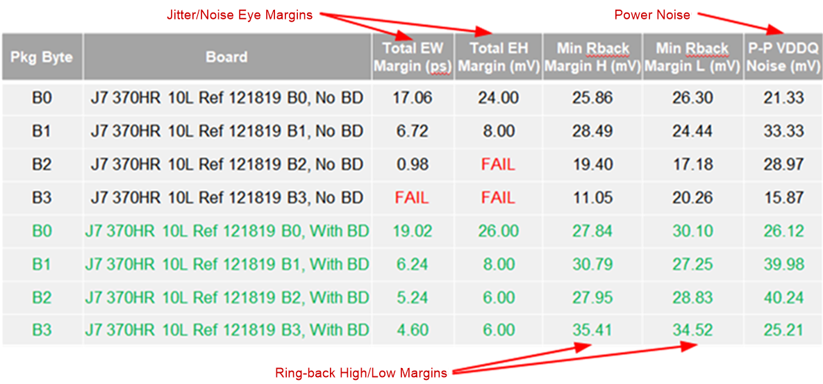
WriteData read simulations need to be verified at SOC. This includes:
- Jitter/noise margins with respect to the eye mask
- Peak-peak power noise
 Figure 4-12 LPDDR4 Simulation Results for
Read
Figure 4-12 LPDDR4 Simulation Results for
ReadThe simulations results for read includes two sets for data, black and green. The black shows the design failed, as several bytes failed to meet the eye margins. The green is the simulation results of the same design, but with back-drilling the via stubs applied.