SPRAD06B March 2022 – November 2024 AM620-Q1 , AM623 , AM625 , AM625-Q1
- 1
- Abstract
- Trademarks
- 1Overview
-
2DDR4 Board Design and Layout Guidance
- 2.1 DDR4 Introduction
- 2.2 DDR4 Device Implementations Supported
- 2.3 DDR4 Interface Schematics
- 2.4 Compatible JEDEC DDR4 Devices
- 2.5 Placement
- 2.6 DDR4 Keepout Region
- 2.7 DBI
- 2.8 VPP
- 2.9 Net Classes
- 2.10 DDR4 Signal Termination
- 2.11 VREF Routing
- 2.12 VTT
- 2.13 POD Interconnect
- 2.14 CK and ADDR_CTRL Topologies and Routing Guidance
- 2.15 Data Group Topologies and Routing Guidance
- 2.16 CK and ADDR_CTRL Routing Specification
- 2.17 Data Group Routing Specification
- 2.18 Bit Swapping
-
3LPDDR4 Board Design and Layout Guidance
- 3.1 LPDDR4 Introduction
- 3.2 LPDDR4 Device Implementations Supported
- 3.3 LPDDR4 Interface Schematics
- 3.4 Compatible JEDEC LPDDR4 Devices
- 3.5 Placement
- 3.6 LPDDR4 Keepout Region
- 3.7 LPDDR4 DBI
- 3.8 Net Classes
- 3.9 LPDDR4 Signal Termination
- 3.10 LPDDR4 VREF Routing
- 3.11 LPDDR4 VTT
- 3.12 CK0 and ADDR_CTRL Topologies
- 3.13 Data Group Topologies
- 3.14 CK0 and ADDR_CTRL Routing Specification
- 3.15 Data Group Routing Specification
- 3.16 Byte and Bit Swapping
- 4LPDDR4 Board Design Simulations
- 5Appendix: AM62x ALW and AMC Package Delays
- 6Revision History
4.5.3.1 Eye Quality
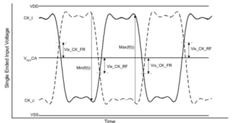
The Vix_DQS ratio and Vix_CK ratio for data write and CA bus simulations are to be verified, at the DRAM pin/BGA. Figure 4-3 from the JEDEC specification explains how to measure the Vix ratio, as well as define the ration requirement(s).
 Figure 4-3 Vix_CK and Vix_DQS Ratio for
Eye Quality
Figure 4-3 Vix_CK and Vix_DQS Ratio for
Eye QualityTable 4-2 Vix_CK and Vix_DQS Ratio for
Eye Quality
| Symbol | Data Rate | Unit | Note | |||||
|---|---|---|---|---|---|---|---|---|
| 1600/1867 | 2133/2400/3200 | 3733/4266 | ||||||
| Vix_CK_ratio | - | 25 | - | 25 | - | 25 | % | (1), (2) |
| Vix_DQS | - | 20 | - | 20 | - | 20 | % | (1), (2) |
(1) Vix_CK_Ratio is defined by the equation: Vix_CK_Ratio =
Vix_CK_FR|Min(f(t))|
(2) Vix_CK_Ratio is defined by the equation: Vix_CK_Ratio =
Vix_CK_RF|Min(f(t))|