SPRAD13A May 2022 – December 2024 AM623 , AM625
- 1
- Abstract
- Trademarks
- 1 Introduction
- 2 Via Channel Arrays
- 3 Width/Spacing Proposal for Escapes
- 4 Stackup
- 5 Via Sharing
- 6 Floorplan Component Placement
- 7 Critical Interfaces Impact Placement
- 8 Routing Priority
- 9 SerDes Interfaces
- 10DDR Interfaces
- 11Power Decoupling
- 12Route Lowest Priority Interfaces Last
- 13Summary
- 14Revision History
10 DDR Interfaces
The AM62 supports connection to both DDR4 and LPDDR4 devices. The DDR signals must be routed next. Refer to the DDR Routing Guidelines document for detailed recommendations for DDR routing. The images below show the BGA breakout for the DDR interface on the AM62 Board. Routing for both DDR4 and LPDDR4 use a similar escape with LPDDR4 requiring lesser number of signals.
The DDR SDRAM memory devices are normally arranged so that the data group balls are closest to the AM62 device. The Package BGA ball map has been carefully planned to place the DDR address and command signals between data byte lane 1 and data byte lane0.
Figure 10-1 and Figure 10-2 show how to escape the DDR byte lanes 0 and 1, respectively. The use of Plated Through Hole (PTH) vias make the routing of these signals between the SoC and SDRAM possible on any layer. An example routing of the DDR data byte lanes on the AM62 SK EVM board is shown in Figure 10-3.
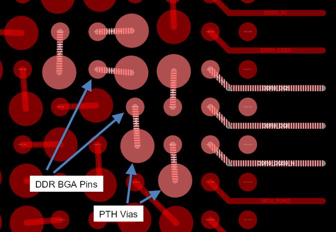 Figure 10-1 DDR Byte Lane0 Escape
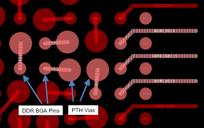 Figure 10-2 DDR Byte Lane1 Escape
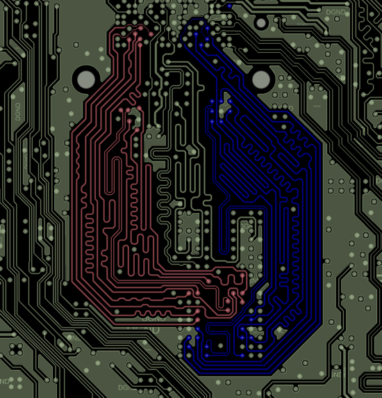 Figure 10-3 DDR Data Byte Lane Routing (Byte Lane0 – Left; Byte Lane1 – Right)
The address, command and clock signals are routed directly to the memory device. This design illustrates routing to a x16 DDR4 memory without VTT termination in a point to point topology. If 2 x8 DDR4 memory devices are used the address, command and clock signals should be routed in a fly-by manner with proper VTT termination.
The top and inner layers escape and route the address and command signals. The traces must be length matched to ensure that the signals arrive at the memory at the same time. Length matching must be from the SoC to memory pin individually and must include the stub to the memory pad and all via lengths. Refer to DDR Routing Guidelines for detailed recommendations for DDR routing.
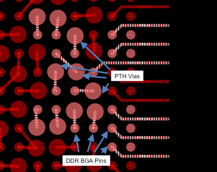 Figure 10-4 DDR Address/Cmd Escape
The escapes of the address and command signals on these layers are shown in Figure 10-4.
Address signals were routed directly from the SoC to the via next to the associated pad for the memory device. This requires that the address signals escape in the correct order. It is required to have the same number of vias for each of the address and command signals. The use of Plated Through Hole (PTH) vias allows the flexibility of routing the address/cmd signals on any layer.
Figure 10-5 shows an example of DDR4 Address, Command, and Clock group routing on the AM62 SK EVM board.
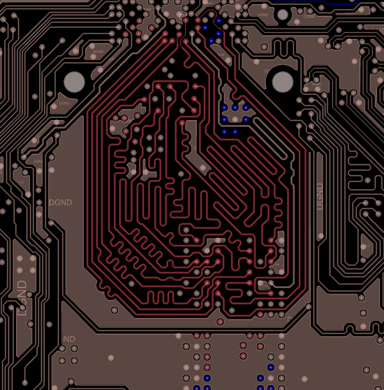 Figure 10-5 DDR4 Address, Command, and Clock Group Routing