SPRAD13A May 2022 – December 2024 AM623 , AM625
- 1
- Abstract
- Trademarks
- 1 Introduction
- 2 Via Channel Arrays
- 3 Width/Spacing Proposal for Escapes
- 4 Stackup
- 5 Via Sharing
- 6 Floorplan Component Placement
- 7 Critical Interfaces Impact Placement
- 8 Routing Priority
- 9 SerDes Interfaces
- 10DDR Interfaces
- 11Power Decoupling
- 12Route Lowest Priority Interfaces Last
- 13Summary
- 14Revision History
2 Via Channel Arrays
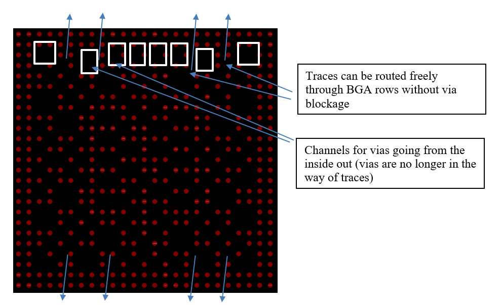
Via Channel Array Technology has been successfully used in a variety of TI products that helps in minimizing package dimensions by using smaller ball pitch and utilizing low cost PCB routing. Via Channel technology is a way of enabling routing channels to escape inner most BGA positions. This allows several advantages. First, the via outside diameter (also known as the annular ring) can be larger than it normally would be if it had to be placed in between the BGA’s in a tighter pitch, since all the vias are placed in special areas called via channels. This makes PCB manufacturing less expensive because larger vias are possible. Second, the vias are grouped in a radial pattern instead of a series of concentric rings around the middle of the chip, which is the case with normal BGA array PCB routing. The traces are more easily routed out of the inner parts of the chip because they are not restricted to the narrow paths in between many rows of vias. The unique outer row routing and the via channel inner routing are two important parts of this technology on the AM62x. The AM62x BGA Via Channel Array is shown in Figure 2-1.
 Figure 2-1 AM62x BGA array with Via Channels
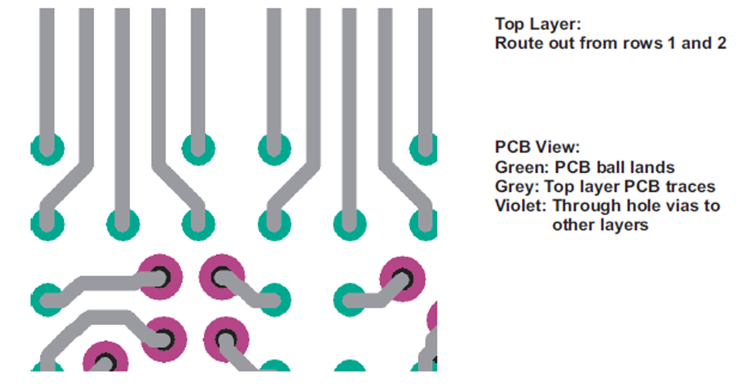
For the first two rows (from the outside in) of the BGA array, the balls have been arranged to allow wider traces than would otherwise be possible. The first row (the outside row) supports any size trace desired, since the trace simply comes from the PCB ball land and goes out on the PCB. Normally, the second row traces must only be routed in between the first row of the PCB ball lands. On this package, however, the second row traces can also be routed through an open channel where the BGA ball has been removed to allow wider traces. The AM62x parts allow a 3.2 mil trace/space in all areas, if routed correctly.
If 3.2 mil wide traces are not able to be supported (wider traces needed), the depopulated BGA in the third row provides added flexibility to allow for the second row to be escaped using a via in this VCA instead of through the first row.
Figure 2-2 shows the first two rows of a VCA package and how it is possible to route large 3.2 mil (mm) traces and spaces in the areas of removed balls.
 Figure 2-2 Outer Rows of Traces
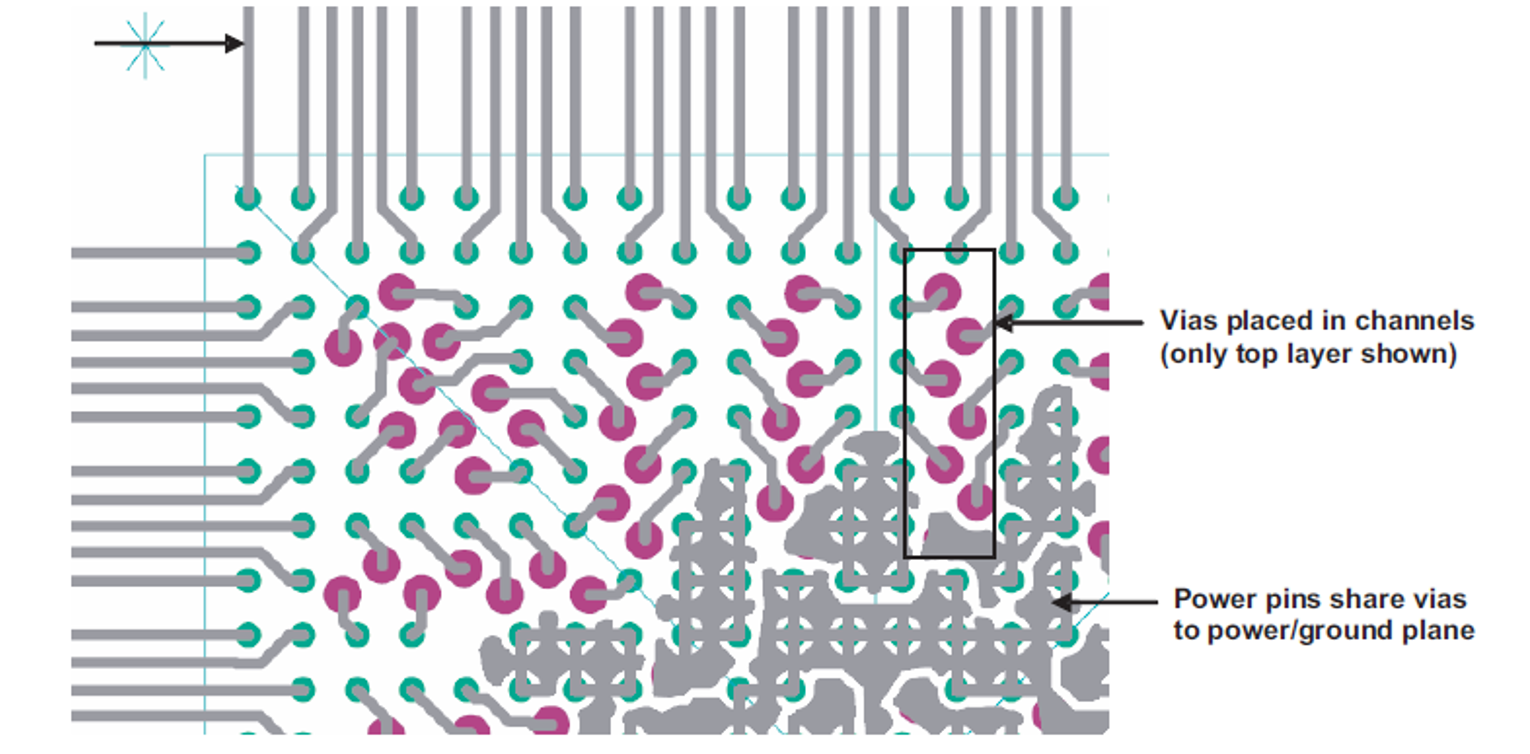
Starting at the third row, as with any BGA package, vias are necessary. As stated before, the vias are gathered in the via channels, so the only vias that need to be placed in between balls are some of the power vias in areas of ground or power copper pour. In this case, they have no regular via ring since they are located in an area of copper pour where all the surrounding balls share the same net. This is elaborated more in the later section with details on via sharing. Since the via ring is larger than one that would normally fit in between these balls with the required clearance, the layout tool may flag a design rule check (DRC) error, however, this is a false warning since there is no risk of shorting to a nearby pad because they are all on the same net. The rest of the vias need to be placed into the via channels as shown below. Figure 2-3 shows how the vias are grouped in the via channels.
 Figure 2-3 Vias in Via Channels