SPRSP58B june   2022  – june 2023 AM620-Q1 , AM623 , AM625 , AM625-Q1

PRODUCTION DATA  

  1.   1
  2. Features
  3. Applications
  4. Description
    1. 3.1 Functional Block Diagram
  5. Revision History
  6. Device Comparison
    1. 5.1 Related Products
  7. Terminal Configuration and Functions
    1. 6.1 Pin Diagrams
    2. 6.2 Pin Attributes
      1.      12
      2.      13
    3. 6.3 Signal Descriptions
      1.      15
      2. 6.3.1  CPSW3G
        1. 6.3.1.1 MAIN Domain
          1.        18
          2.        19
          3.        20
          4.        21
      3. 6.3.2  CPTS
        1. 6.3.2.1 MAIN Domain
          1.        24
      4. 6.3.3  CSI-2
        1. 6.3.3.1 MAIN Domain
          1.        27
      5. 6.3.4  DDRSS
        1. 6.3.4.1 MAIN Domain
          1.        30
      6. 6.3.5  DSS
        1. 6.3.5.1 MAIN Domain
          1.        33
      7. 6.3.6  ECAP
        1. 6.3.6.1 MAIN Domain
          1.        36
          2.        37
          3.        38
      8. 6.3.7  Emulation and Debug
        1. 6.3.7.1 MAIN Domain
          1.        41
        2. 6.3.7.2 MCU Domain
          1.        43
      9. 6.3.8  EPWM
        1. 6.3.8.1 MAIN Domain
          1.        46
          2.        47
          3.        48
          4.        49
      10. 6.3.9  EQEP
        1. 6.3.9.1 MAIN Domain
          1.        52
          2.        53
          3.        54
      11. 6.3.10 GPIO
        1. 6.3.10.1 MAIN Domain
          1.        57
          2.        58
        2. 6.3.10.2 MCU Domain
          1.        60
      12. 6.3.11 GPMC
        1. 6.3.11.1 MAIN Domain
          1.        63
      13. 6.3.12 I2C
        1. 6.3.12.1 MAIN Domain
          1.        66
          2.        67
          3.        68
          4.        69
        2. 6.3.12.2 MCU Domain
          1.        71
        3. 6.3.12.3 WKUP Domain
          1.        73
      14. 6.3.13 MCAN
        1. 6.3.13.1 MAIN Domain
          1.        76
        2. 6.3.13.2 MCU Domain
          1.        78
          2.        79
      15. 6.3.14 MCASP
        1. 6.3.14.1 MAIN Domain
          1.        82
          2.        83
          3.        84
      16. 6.3.15 MCSPI
        1. 6.3.15.1 MAIN Domain
          1.        87
          2.        88
          3.        89
        2. 6.3.15.2 MCU Domain
          1.        91
          2.        92
      17. 6.3.16 MDIO
        1. 6.3.16.1 MAIN Domain
          1.        95
      18. 6.3.17 MMC
        1. 6.3.17.1 MAIN Domain
          1.        98
          2.        99
          3.        100
      19. 6.3.18 OLDI
        1. 6.3.18.1 MAIN Domain
          1.        103
      20. 6.3.19 OSPI
        1. 6.3.19.1 MAIN Domain
          1.        106
      21. 6.3.20 Power Supply
        1.       108
      22. 6.3.21 PRUSS
        1. 6.3.21.1 MAIN Domain
          1.        111
          2.        112
      23. 6.3.22 Reserved
        1.       114
      24. 6.3.23 System and Miscellaneous
        1. 6.3.23.1 Boot Mode Configuration
          1. 6.3.23.1.1 MAIN Domain
            1.         118
        2. 6.3.23.2 Clock
          1. 6.3.23.2.1 MCU Domain
            1.         121
          2. 6.3.23.2.2 WKUP Domain
            1.         123
        3. 6.3.23.3 System
          1. 6.3.23.3.1 MAIN Domain
            1.         126
          2. 6.3.23.3.2 MCU Domain
            1.         128
          3. 6.3.23.3.3 WKUP Domain
            1.         130
        4. 6.3.23.4 VMON
          1.        132
      25. 6.3.24 TIMER
        1. 6.3.24.1 MAIN Domain
          1.        135
        2. 6.3.24.2 MCU Domain
          1.        137
        3. 6.3.24.3 WKUP Domain
          1.        139
      26. 6.3.25 UART
        1. 6.3.25.1 MAIN Domain
          1.        142
          2.        143
          3.        144
          4.        145
          5.        146
          6.        147
          7.        148
        2. 6.3.25.2 MCU Domain
          1.        150
        3. 6.3.25.3 WKUP Domain
          1.        152
      27. 6.3.26 USB
        1. 6.3.26.1 MAIN Domain
          1.        155
          2.        156
    4. 6.4 Pin Connectivity Requirements
  8. Specifications
    1. 7.1  Absolute Maximum Ratings
    2. 7.2  ESD Ratings for Devices which are not AEC - Q100 Qualified
    3. 7.3  ESD Ratings for AEC - Q100 Qualified Devices in the AMC Package
    4. 7.4  Power-On Hours (POH)
    5. 7.5  Recommended Operating Conditions
    6. 7.6  Operating Performance Points
    7. 7.7  Power Consumption Summary
    8. 7.8  Electrical Characteristics
      1. 7.8.1  I2C Open-Drain, and Fail-Safe (I2C OD FS) Electrical Characteristics
      2. 7.8.2  Fail-Safe Reset (FS RESET) Electrical Characteristics
      3. 7.8.3  High-Frequency Oscillator (HFOSC) Electrical Characteristics
      4. 7.8.4  Low-Frequency Oscillator (LFXOSC) Electrical Characteristics
      5. 7.8.5  SDIO Electrical Characteristics
      6. 7.8.6  LVCMOS Electrical Characteristics
      7. 7.8.7  OLDI LVDS (OLDI) Electrical Characteristics
      8. 7.8.8  CSI-2 (D-PHY) Electrical Characteristics
      9. 7.8.9  USB2PHY Electrical Characteristics
      10. 7.8.10 DDR Electrical Characteristics
    9. 7.9  VPP Specifications for One-Time Programmable (OTP) eFuses
      1. 7.9.1 Recommended Operating Conditions for OTP eFuse Programming
      2. 7.9.2 Hardware Requirements
      3. 7.9.3 Programming Sequence
      4. 7.9.4 Impact to Your Hardware Warranty
    10. 7.10 Thermal Resistance Characteristics
      1. 7.10.1 Thermal Resistance Characteristics for ALW and AMC Packages
    11. 7.11 Timing and Switching Characteristics
      1. 7.11.1 Timing Parameters and Information
      2. 7.11.2 Power Supply Requirements
        1. 7.11.2.1 Power Supply Slew Rate Requirement
        2. 7.11.2.2 Power Supply Sequencing
          1. 7.11.2.2.1 Power-Up Sequencing
          2. 7.11.2.2.2 Power-Down Sequencing
          3. 7.11.2.2.3 Partial IO Power Sequencing
      3. 7.11.3 System Timing
        1. 7.11.3.1 Reset Timing
        2. 7.11.3.2 Error Signal Timing
        3. 7.11.3.3 Clock Timing
      4. 7.11.4 Clock Specifications
        1. 7.11.4.1 Input Clocks / Oscillators
          1. 7.11.4.1.1 MCU_OSC0 Internal Oscillator Clock Source
            1. 7.11.4.1.1.1 Load Capacitance
            2. 7.11.4.1.1.2 Shunt Capacitance
          2. 7.11.4.1.2 MCU_OSC0 LVCMOS Digital Clock Source
          3. 7.11.4.1.3 WKUP_LFOSC0 Internal Oscillator Clock Source
          4. 7.11.4.1.4 WKUP_LFOSC0 LVCMOS Digital Clock Source
          5. 7.11.4.1.5 WKUP_LFOSC0 Not Used
        2. 7.11.4.2 Output Clocks
        3. 7.11.4.3 PLLs
        4. 7.11.4.4 Recommended System Precautions for Clock and Control Signal Transitions
      5. 7.11.5 Peripherals
        1. 7.11.5.1  CPSW3G
          1. 7.11.5.1.1 CPSW3G MDIO Timing
          2. 7.11.5.1.2 CPSW3G RMII Timing
          3. 7.11.5.1.3 CPSW3G RGMII Timing
        2. 7.11.5.2  CPTS
        3. 7.11.5.3  CSI-2
        4. 7.11.5.4  DDRSS
        5. 7.11.5.5  DSS
        6. 7.11.5.6  ECAP
        7. 7.11.5.7  Emulation and Debug
          1. 7.11.5.7.1 Trace
          2. 7.11.5.7.2 JTAG
        8. 7.11.5.8  EPWM
        9. 7.11.5.9  EQEP
        10. 7.11.5.10 GPIO
        11. 7.11.5.11 GPMC
          1. 7.11.5.11.1 GPMC and NOR Flash — Synchronous Mode
          2. 7.11.5.11.2 GPMC and NOR Flash — Asynchronous Mode
          3. 7.11.5.11.3 GPMC and NAND Flash — Asynchronous Mode
        12. 7.11.5.12 I2C
        13. 7.11.5.13 MCAN
        14. 7.11.5.14 MCASP
        15. 7.11.5.15 MCSPI
          1. 7.11.5.15.1 MCSPI — Controller Mode
          2. 7.11.5.15.2 MCSPI — Peripheral Mode
        16. 7.11.5.16 MMCSD
          1. 7.11.5.16.1 MMC0 - eMMC/SD/SDIO Interface
            1. 7.11.5.16.1.1  Legacy SDR Mode
            2. 7.11.5.16.1.2  High Speed SDR Mode
            3. 7.11.5.16.1.3  HS200 Mode
            4. 7.11.5.16.1.4  Default Speed Mode
            5. 7.11.5.16.1.5  High Speed Mode
            6. 7.11.5.16.1.6  UHS–I SDR12 Mode
            7. 7.11.5.16.1.7  UHS–I SDR25 Mode
            8. 7.11.5.16.1.8  UHS–I SDR50 Mode
            9. 7.11.5.16.1.9  UHS–I DDR50 Mode
            10. 7.11.5.16.1.10 UHS–I SDR104 Mode
          2. 7.11.5.16.2 MMC1/MMC2 - SD/SDIO Interface
            1. 7.11.5.16.2.1 Default Speed Mode
            2. 7.11.5.16.2.2 High Speed Mode
            3. 7.11.5.16.2.3 UHS–I SDR12 Mode
            4. 7.11.5.16.2.4 UHS–I SDR25 Mode
            5. 7.11.5.16.2.5 UHS–I SDR50 Mode
            6. 7.11.5.16.2.6 UHS–I DDR50 Mode
            7. 7.11.5.16.2.7 UHS–I SDR104 Mode
        17. 7.11.5.17 OLDI
          1. 7.11.5.17.1 OLDI0 Switching Characteristics
        18. 7.11.5.18 OSPI
          1. 7.11.5.18.1 OSPI0 PHY Mode
            1. 7.11.5.18.1.1 OSPI0 With PHY Data Training
            2. 7.11.5.18.1.2 OSPI0 Without Data Training
              1. 7.11.5.18.1.2.1 OSPI0 PHY SDR Timing
              2. 7.11.5.18.1.2.2 OSPI0 PHY DDR Timing
          2. 7.11.5.18.2 OSPI0 Tap Mode
            1. 7.11.5.18.2.1 OSPI0 Tap SDR Timing
            2. 7.11.5.18.2.2 OSPI0 Tap DDR Timing
        19. 7.11.5.19 PRUSS
          1. 7.11.5.19.1 PRUSS Programmable Real-Time Unit (PRU)
            1. 7.11.5.19.1.1 PRUSS PRU Direct Output Mode Timing
            2. 7.11.5.19.1.2 PRUSS PRU Parallel Capture Mode Timing
            3. 7.11.5.19.1.3 PRUSS PRU Shift Mode Timing
          2. 7.11.5.19.2 PRUSS Industrial Ethernet Peripheral (IEP)
            1. 7.11.5.19.2.1 PRUSS IEP Timing
          3. 7.11.5.19.3 PRUSS Universal Asynchronous Receiver Transmitter (UART)
            1. 7.11.5.19.3.1 PRUSS UART Timing
          4. 7.11.5.19.4 PRUSS Enhanced Capture Peripheral (ECAP)
            1. 7.11.5.19.4.1 PRUSS ECAP Timing
        20. 7.11.5.20 Timers
        21. 7.11.5.21 UART
        22. 7.11.5.22 USB
  9. Detailed Description
    1. 8.1 Overview
    2. 8.2 Processor Subsystems
      1. 8.2.1 Arm Cortex-A53 Subsystem
      2. 8.2.2 Device/Power Manager
      3. 8.2.3 Arm Cortex-M4F
    3. 8.3 Accelerators and Coprocessors
      1. 8.3.1 Graphics Processing Unit (GPU)
      2. 8.3.2 Programmable Real-Time Unit Subsystem (PRUSS)
    4. 8.4 Other Subsystems
      1. 8.4.1 Dual Clock Comparator (DCC)
      2. 8.4.2 Data Movement Subsystem (DMSS)
      3. 8.4.3 Memory Cyclic Redundancy Check (MCRC)
      4. 8.4.4 Peripheral DMA Controller (PDMA)
      5. 8.4.5 Real-Time Clock (RTC)
    5. 8.5 Peripherals
      1. 8.5.1  Gigabit Ethernet Switch (CPSW3G)
      2. 8.5.2  Camera Streaming Interface Receiver (CSI_RX_IF)
      3. 8.5.3  DDR Subsystem (DDRSS)
      4. 8.5.4  Display Subsystem (DSS)
      5. 8.5.5  Enhanced Capture (ECAP)
      6. 8.5.6  Error Location Module (ELM)
      7. 8.5.7  Enhanced Pulse Width Modulation (EPWM)
      8. 8.5.8  Error Signaling Module (ESM)
      9. 8.5.9  Enhanced Quadrature Encoder Pulse (EQEP)
      10. 8.5.10 General-Purpose Interface (GPIO)
      11. 8.5.11 General-Purpose Memory Controller (GPMC)
      12. 8.5.12 Global Timebase Counter (GTC)
      13. 8.5.13 Inter-Integrated Circuit (I2C)
      14. 8.5.14 Modular Controller Area Network (MCAN)
      15. 8.5.15 Multichannel Audio Serial Port (MCASP)
      16. 8.5.16 Multichannel Serial Peripheral Interface (MCSPI)
      17. 8.5.17 Multi-Media Card Secure Digital (MMCSD)
      18. 8.5.18 Octal Serial Peripheral Interface (OSPI)
      19. 8.5.19 Timers
      20. 8.5.20 Universal Asynchronous Receiver/Transmitter (UART)
      21. 8.5.21 Universal Serial Bus Subsystem (USBSS)
  10. Applications, Implementation, and Layout
    1. 9.1 Device Connection and Layout Fundamentals
      1. 9.1.1 Power Supply
        1. 9.1.1.1 Power Supply Designs
        2. 9.1.1.2 Power Distribution Network Implementation Guidance
      2. 9.1.2 External Oscillator
      3. 9.1.3 JTAG, EMU, and TRACE
      4. 9.1.4 Reset
      5. 9.1.5 Unused Pins
    2. 9.2 Peripheral- and Interface-Specific Design Information
      1. 9.2.1 DDR Board Design and Layout Guidelines
      2. 9.2.2 OSPI/QSPI/SPI Board Design and Layout Guidelines
        1. 9.2.2.1 No Loopback, Internal PHY Loopback, and Internal Pad Loopback
        2. 9.2.2.2 External Board Loopback
        3. 9.2.2.3 DQS (only available in Octal SPI devices)
      3. 9.2.3 USB VBUS Design Guidelines
      4. 9.2.4 System Power Supply Monitor Design Guidelines
      5. 9.2.5 High Speed Differential Signal Routing Guidance
      6. 9.2.6 Thermal Solution Guidance
  11. 10Device and Documentation Support
    1. 10.1 Device Nomenclature
      1. 10.1.1 Standard Package Symbolization
      2. 10.1.2 Device Naming Convention
    2. 10.2 Tools and Software
    3. 10.3 Documentation Support
    4. 10.4 Support Resources
    5. 10.5 Trademarks
    6. 10.6 Electrostatic Discharge Caution
    7. 10.7 Glossary
  12. 11Mechanical, Packaging, and Orderable Information
    1. 11.1 Packaging Information
WKUP_LFOSC0 Internal Oscillator Clock Source

Figure 7-21 shows the recommended crystal circuit. It is recommended that preproduction printed-circuit board (PCB) designs include the two optional resistors Rbias and Rd in case they are required for proper oscillator operation when combined with production crystal circuit components. In most cases, Rbias is not required and Rd is a 0-Ω resistor. These resistors may be removed from production PCB designs after evaluating oscillator performance with production crystal circuit components installed on preproduction PCBs.
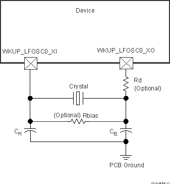
GUID-515F6483-F4C9-4689-9862-659B08781F4F-low.gif Figure 7-21 WKUP_LFOSC0 Crystal Implementation

Table 7-23 presents LFXOSC modes of operation.

Table 7-23 LFXOSC Modes of Operation
MODE BP_C PD_C XI XO CLK_OUT DESCRIPTION
ACTIVE 0 0 XTAL XTAL CLK_OUT Active oscillator mode providing 32kHz
PWRDN 0 1 X PD LOW Output will be pulled down to LOW. PAD to be tri-stated. Active mode disabled
BYPASS 1 0 CLK PD CLK XI is driven by external clock source. XO is pulled down to LOW. Due to ESD diode to supply, XI should not be driven unless oscillator supply is present.
Note:

User should set CTRLMMR_WKUP_LFXOSC_TRIM[18:16] i_mult = 3b’001 for CL in the range 6pf to 9.5pf. CTRLMMR_WKUP_LFXOSC_TRIM [18:16] i_mult = 3b’010 for CL in the range 8.5pf to 12pf. Default setting is 3b’010.

Note:

The load capacitors, Cf1 and Cf2 in Figure 7-22, should be chosen such that the below equation is satisfied. CL in the equation is the load specified by the crystal manufacturer. All discrete components used to implement the oscillator circuit should be placed as close as possible to the associated oscillator WKUP_LFOSC0_XI, WKUP_LFOSC0_XO, and VSS pins.

GUID-A11F106E-2A47-4412-86B0-F2B1F29E7A80-low.gif Figure 7-22 Load Capacitance Equation

The crystal must be in the fundamental mode of operation and parallel resonant. Table 7-24 summarizes the required electrical constraints.

Table 7-24 WKUP_LFOSC0 Crystal Electrical Characteristics
NAME DESCRIPTION MIN TYP MAX UNIT
fp Parallel resonance crystal frequency 32768 Hz
Cf1 Cf1 load capacitance for crystal parallel resonance with Cf1 = Cf2 12 24 pF
Cf2 Cf2 load capacitance for crystal parallel resonance with Cf1 = Cf2 12 24 pF
Cshunt Shunt capacitance ESRxtal – 40 kΩ 4 pF
ESRxtal – 60 kΩ 3 pF
ESRxtal – 80 kΩ 2 pF
ESRxtal – 100 kΩ 1 pF
ESR Crystal effective series resistance (1) Ω
The maximum ESR of the crystal is a function of the crystal frequency and shunt capacitance. See the Cshunt parameter.

When selecting a crystal, the system design must consider the temperature and aging characteristics of a based on the worst case environment and expected life expectancy of the system.

Table 7-25 details the switching characteristics of the oscillator and the requirements of the input clock.

Table 7-25 WKUP_LFOSC0 Switching Characteristics – Crystal Mode
NAME DESCRIPTION MIN TYP MAX UNIT
fxtal Oscillation frequency 32768 Hz
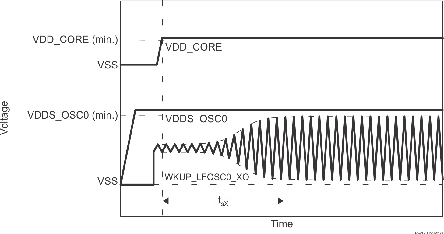
tsX Start-up time 96.5 ms
GUID-20221021-SS0I-HCN3-1BNH-VC99HZ0F2LRP-low.gif Figure 7-23 WKUP_LFOSC0 Start-up Time