SPRSPA7A September   2024  – November 2024 AM2612

ADVANCE INFORMATION  

  1.   1
  2. Features
  3. Applications
  4. Description
    1. 3.1 Functional Block Diagram
  5. Package Comparison
    1. 4.1 Related Products
  6. Terminal Configuration and Functions
    1. 5.1 Pin Diagram
      1. 5.1.1 AM261x ZCZ Pin Diagram
      2. 5.1.2 AM261x ZFG Pin Diagram
      3. 5.1.3 AM261x ZEJ Pin Diagram
      4. 5.1.4 AM261x ZNC Pin Diagram
    2. 5.2 Pin Attributes
      1.      15
      2.      16
    3. 5.3 Signal Descriptions
      1.      18
      2. 5.3.1  ADC
        1.       20
        2.       21
        3.       22
      3. 5.3.2  ADC_CAL
        1.       24
      4. 5.3.3  ADC VREF
        1.       26
      5. 5.3.4  CPSW
        1.       28
        2.       29
        3.       30
        4.       31
        5.       32
        6.       33
        7.       34
      6. 5.3.5  CPTS
        1.       36
      7. 5.3.6  DAC
        1.       38
      8. 5.3.7  EPWM
        1.       40
        2.       41
        3.       42
        4.       43
        5.       44
        6.       45
        7.       46
        8.       47
        9.       48
        10.       49
      9. 5.3.8  EQEP
        1.       51
        2.       52
      10. 5.3.9  FSI
        1.       54
        2.       55
      11. 5.3.10 GPIO
        1.       57
      12. 5.3.11 GPMC0
        1.       59
      13. 5.3.12 I2C
        1.       61
        2.       62
        3.       63
      14. 5.3.13 LIN
        1.       65
        2.       66
        3.       67
      15. 5.3.14 MCAN
        1.       69
        2.       70
      16. 5.3.15 SPI (MCSPI)
        1.       72
        2.       73
        3.       74
        4.       75
      17. 5.3.16 MMC
        1.       77
      18. 5.3.17 Power Supply
        1.       79
      19. 5.3.18 PRU-ICSS
        1.       81
        2.       82
        3.       83
        4.       84
        5.       85
      20. 5.3.19 OSPI
        1.       87
        2.       88
      21. 5.3.20 SDFM
        1.       90
        2.       91
      22. 5.3.21 System and Miscellaneous
        1. 5.3.21.1 Boot Mode Configuration
          1.        94
        2. 5.3.21.2 Clocking
          1.        96
          2.        97
          3.        98
        3. 5.3.21.3 Emulation and Debug
          1.        100
          2.        101
        4. 5.3.21.4 SYSTEM
          1.        103
        5. 5.3.21.5 USB0
          1.        105
        6. 5.3.21.6 VMON
          1.        107
        7.       108
          1.        109
      23. 5.3.22 UART
        1.       111
        2.       112
        3.       113
        4.       114
        5.       115
        6.       116
      24. 5.3.23 XBAR
        1.       118
        2.       119
  7. Specifications
    1. 6.1 Absolute Maximum Ratings
    2. 6.2 Recommended Operating Conditions
    3. 6.3 Electrical Characteristics
      1. 6.3.1 Digital and Analog IO Electrical Characteristics
    4. 6.4 Thermal Resistance Characteristics
      1. 6.4.1 Package Thermal Characteristics
  8. Detailed Description
    1. 7.1 Overview
    2. 7.2 Processor Subsystems
      1. 7.2.1 Arm Cortex-R5F Subsystem
  9. Applications, Implementation, and Layout
    1. 8.1 Device Connection and Layout Fundamentals
      1. 8.1.1 External Oscillator
      2. 8.1.2 JTAG, EMU, and TRACE
      3. 8.1.3 Hardware Reference Design and Guidelines
  10. Device and Documentation Support
    1. 9.1 Device Nomenclature
      1. 9.1.1 Device Naming Convention
    2. 9.2 Tools and Software
    3. 9.3 Documentation Support
    4. 9.4 Support Resources
    5. 9.5 Trademarks
    6. 9.6 Electrostatic Discharge Caution
    7. 9.7 Glossary
  11. 10Revision History
  12. 11Mechanical, Packaging, and Orderable Information

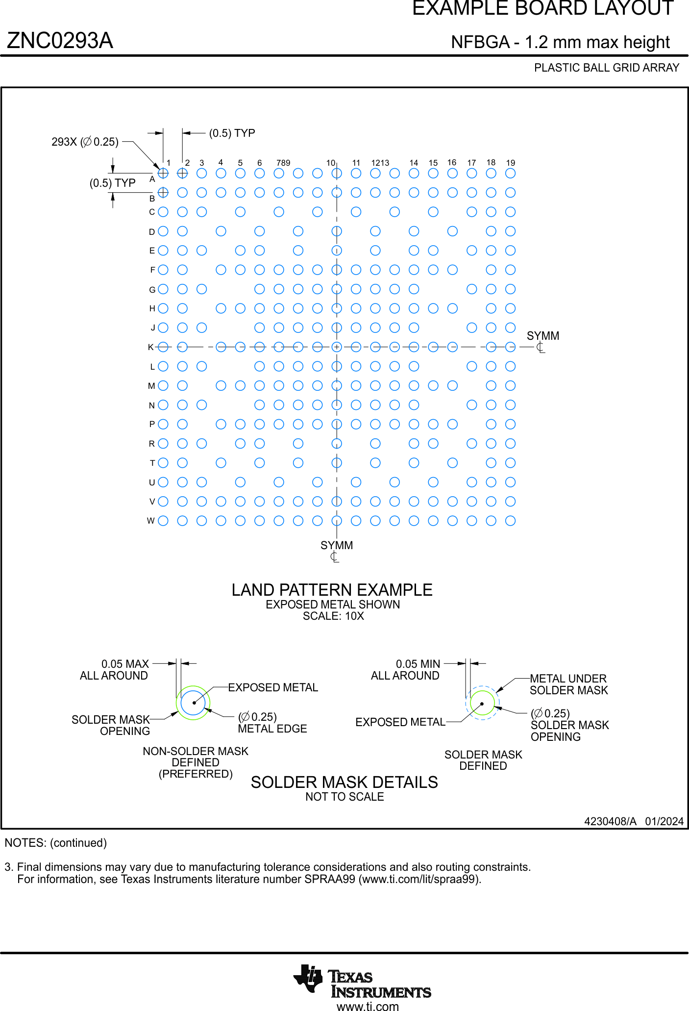
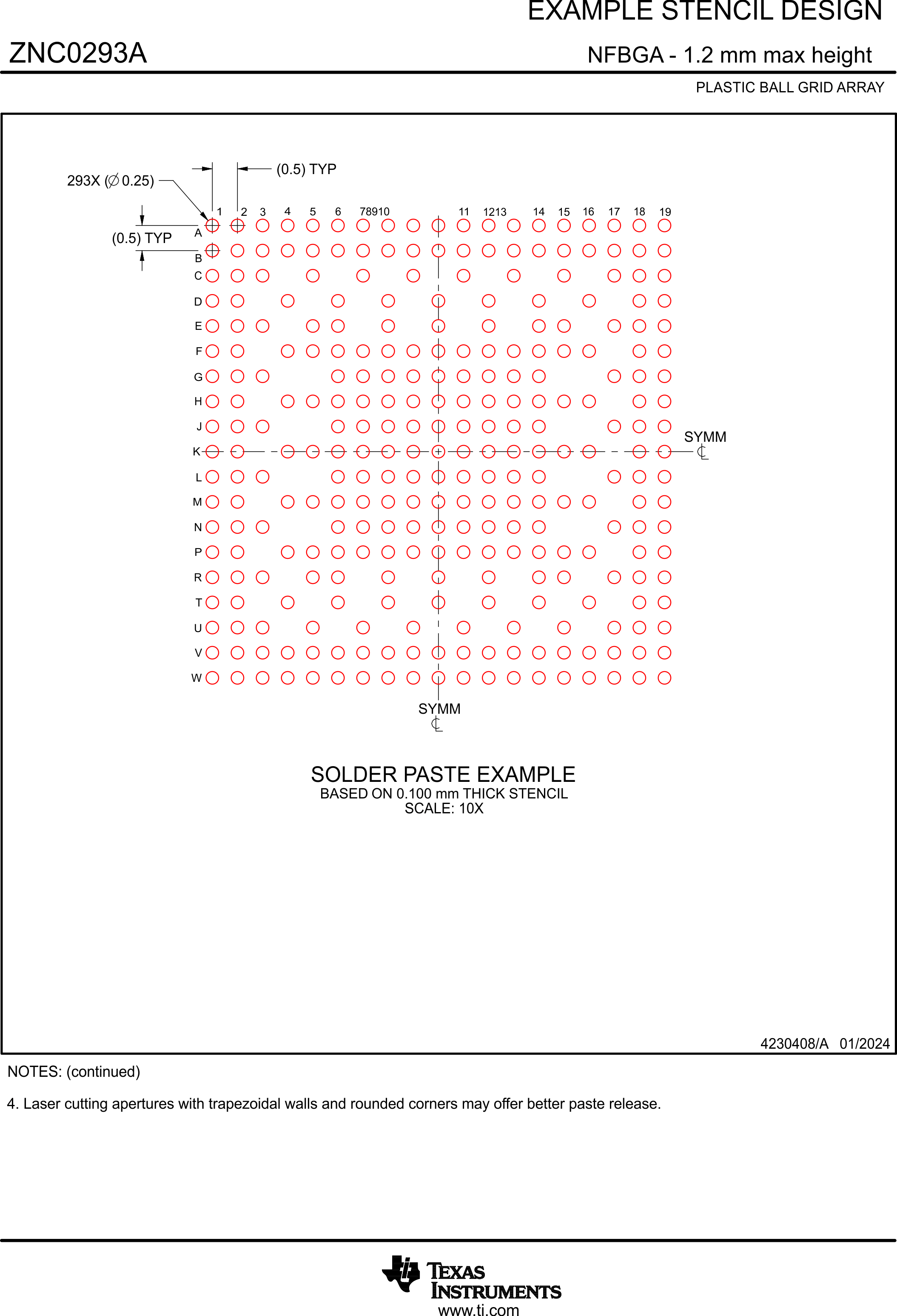
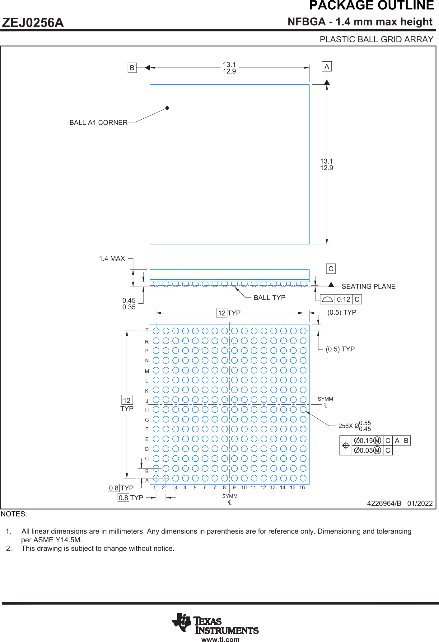
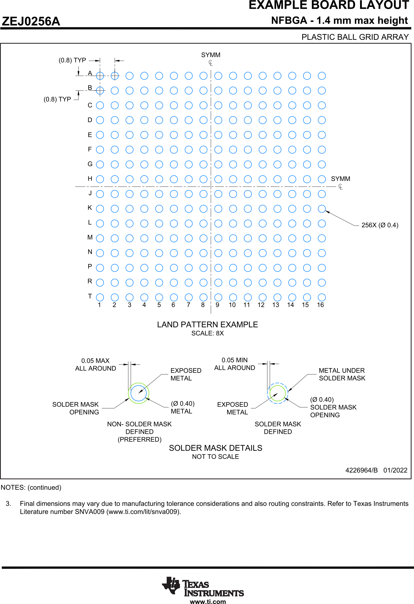
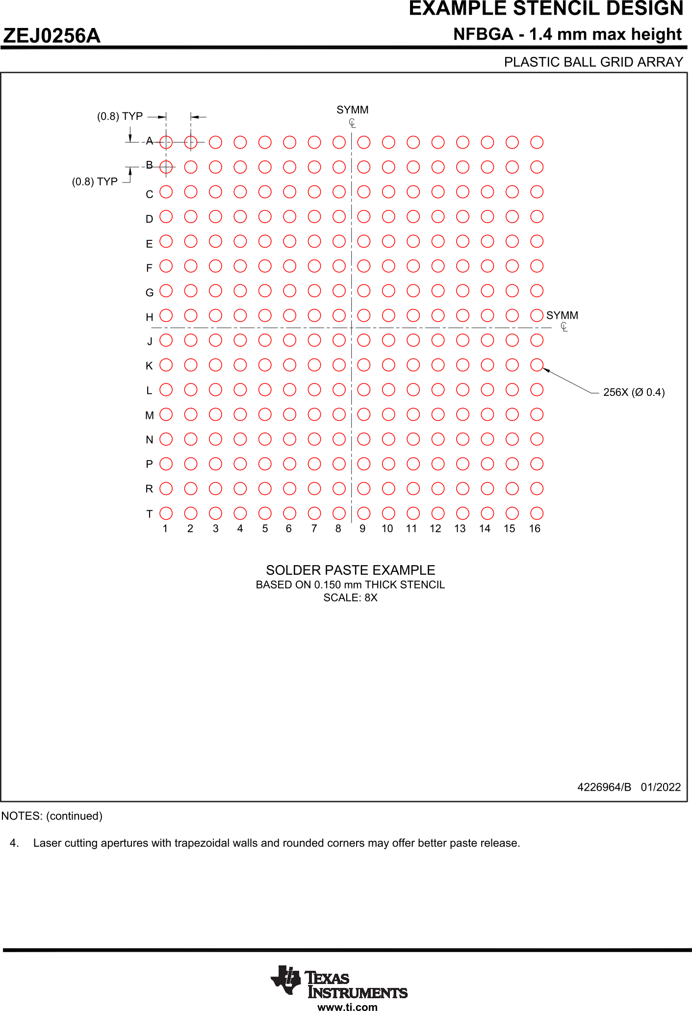
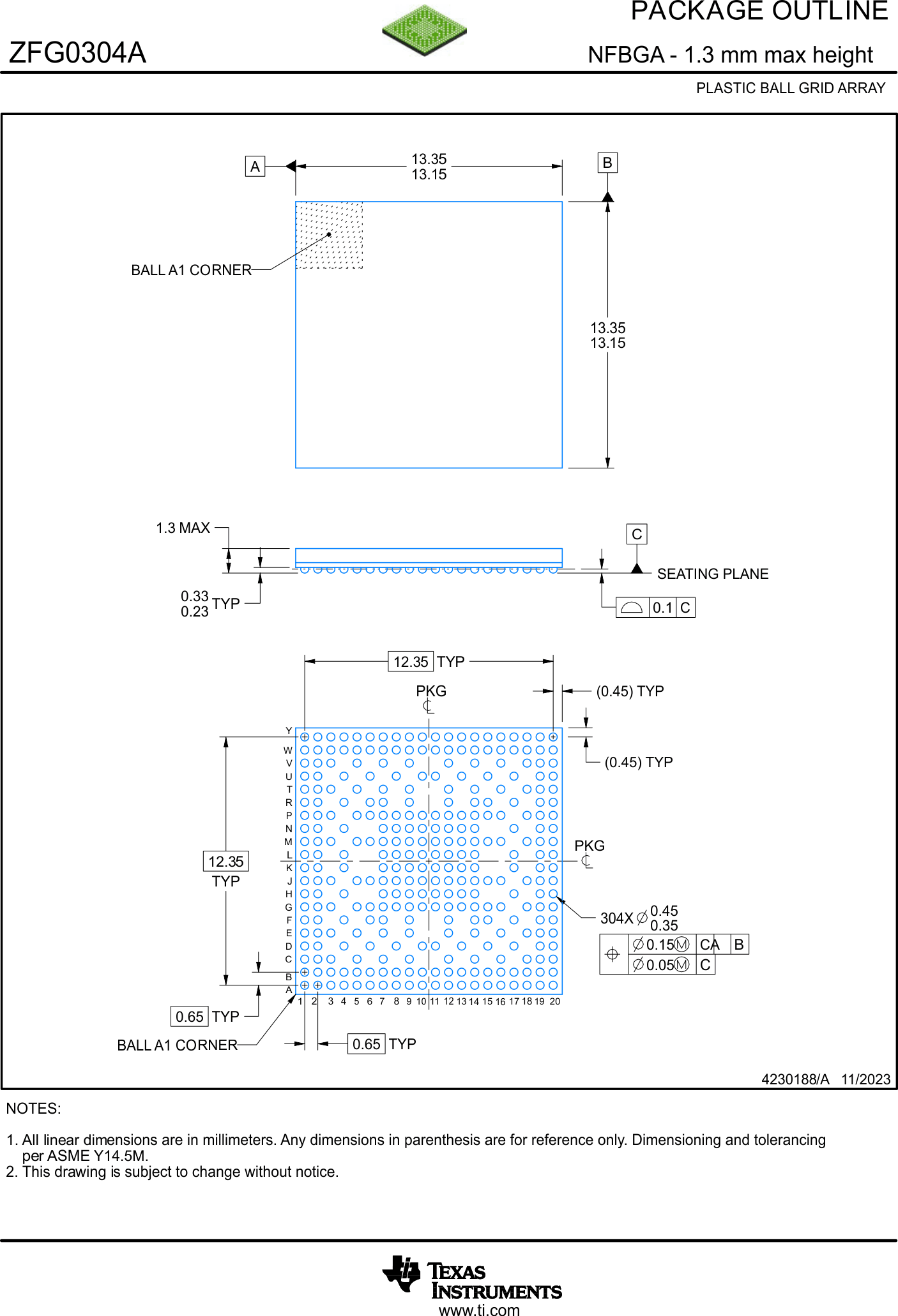
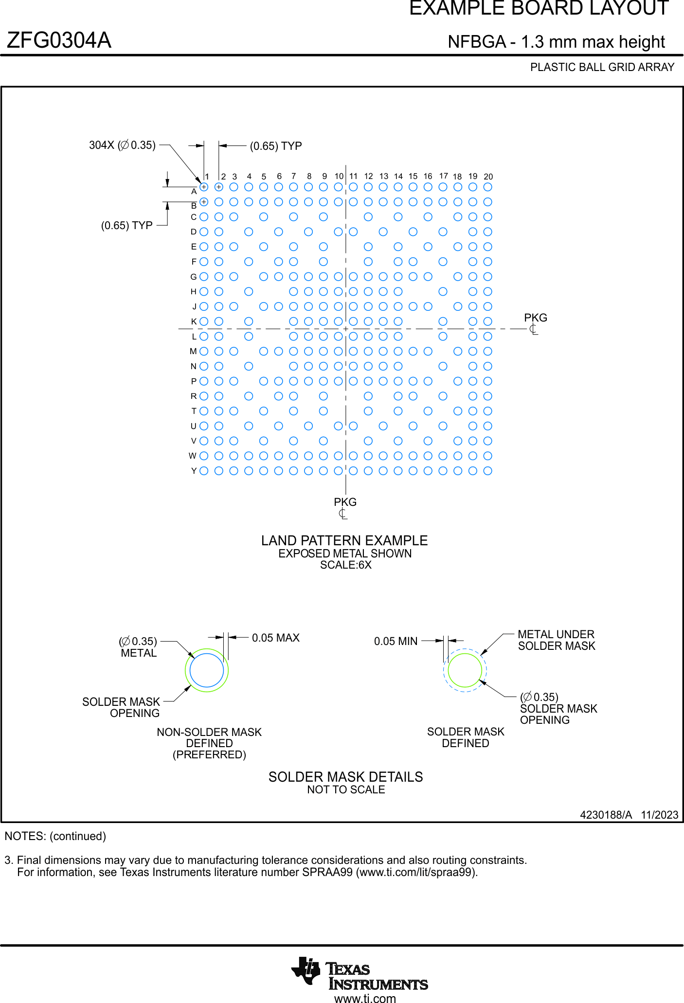
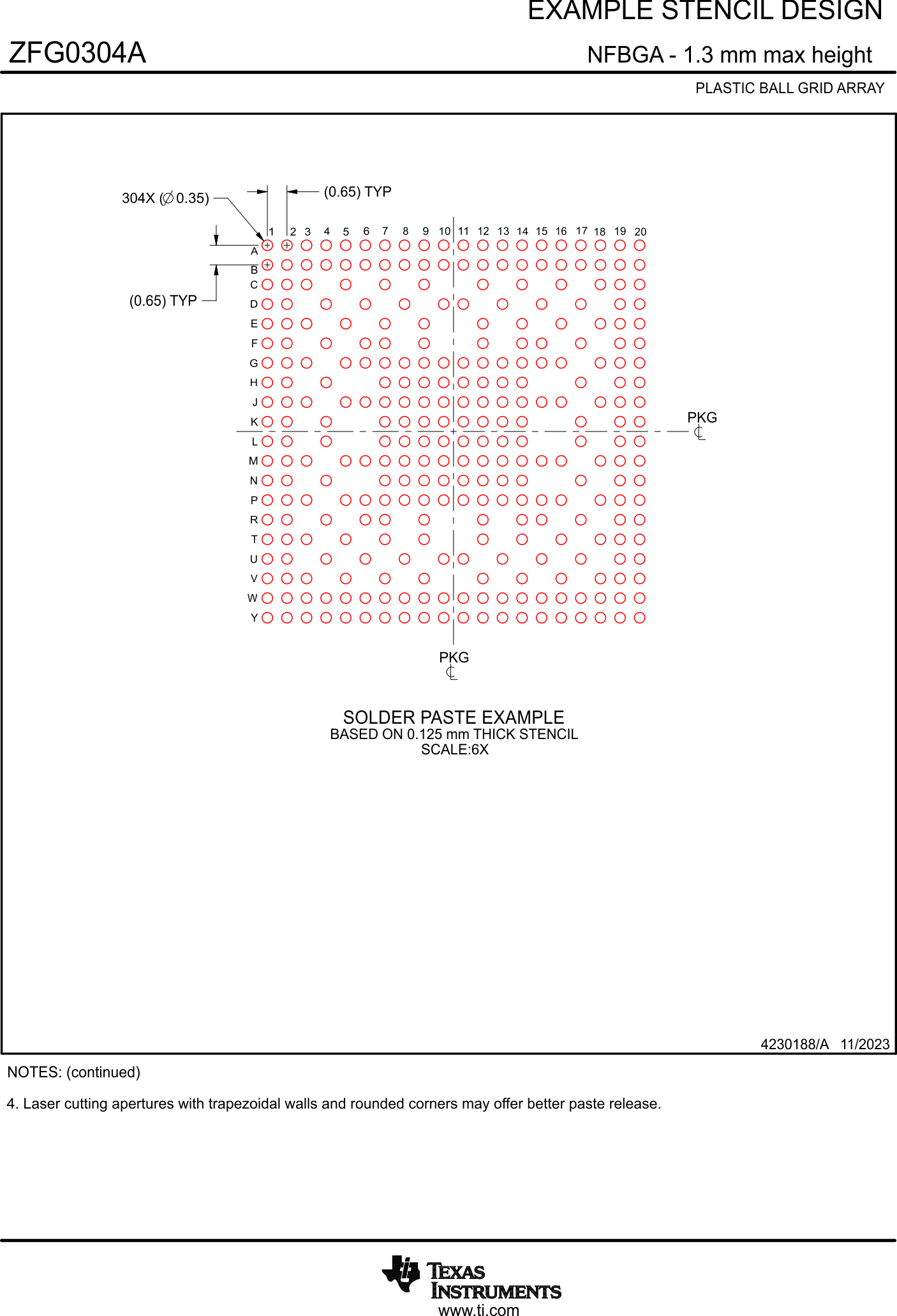
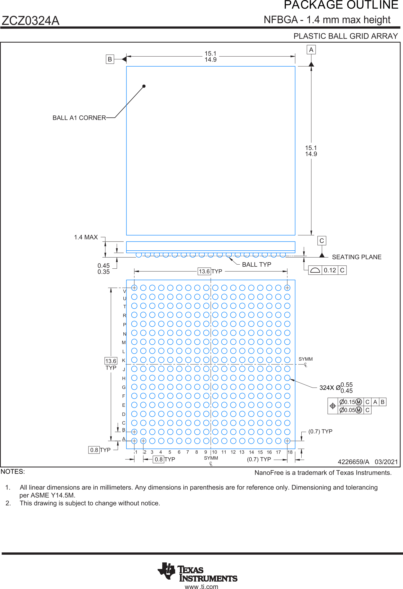
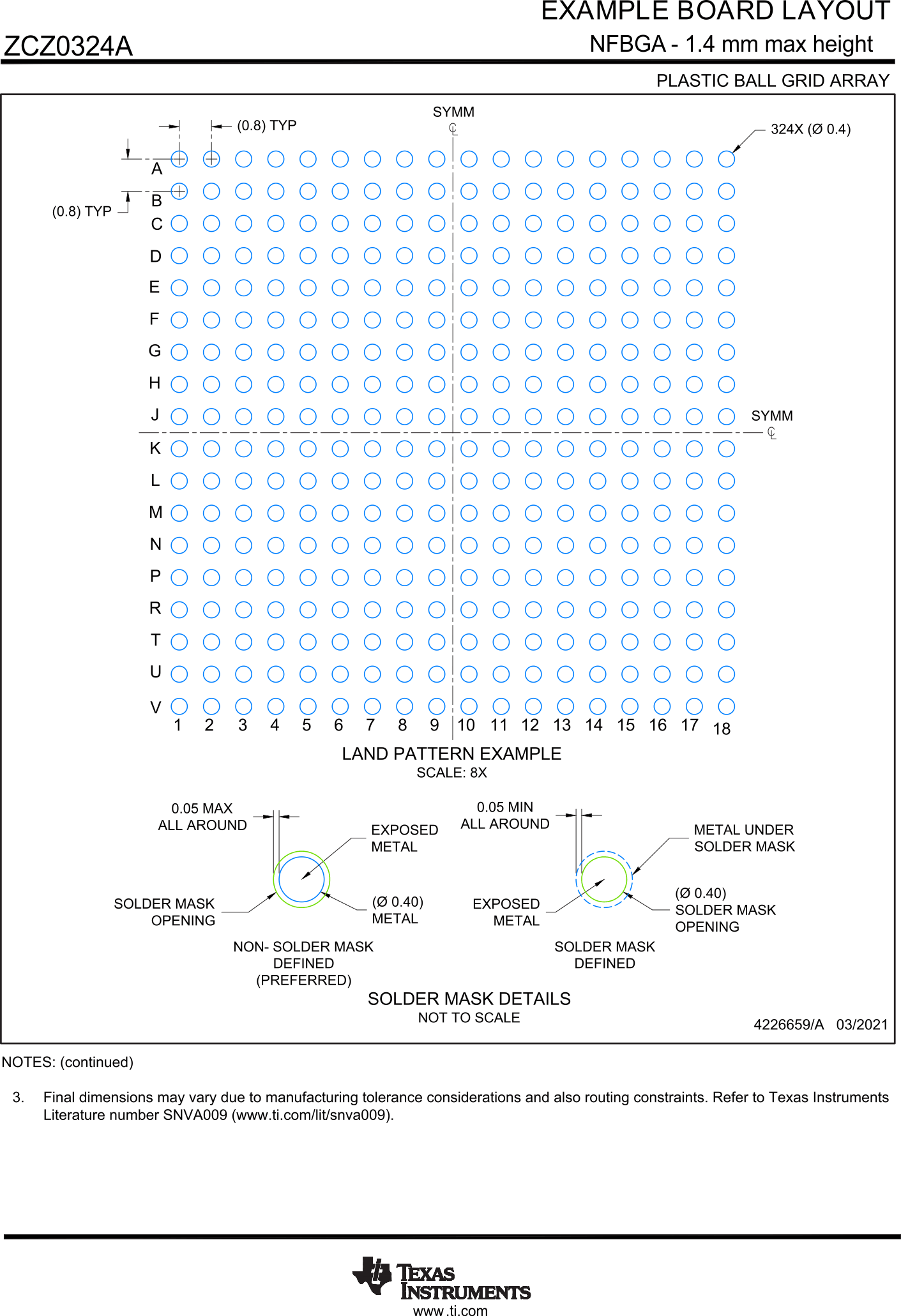
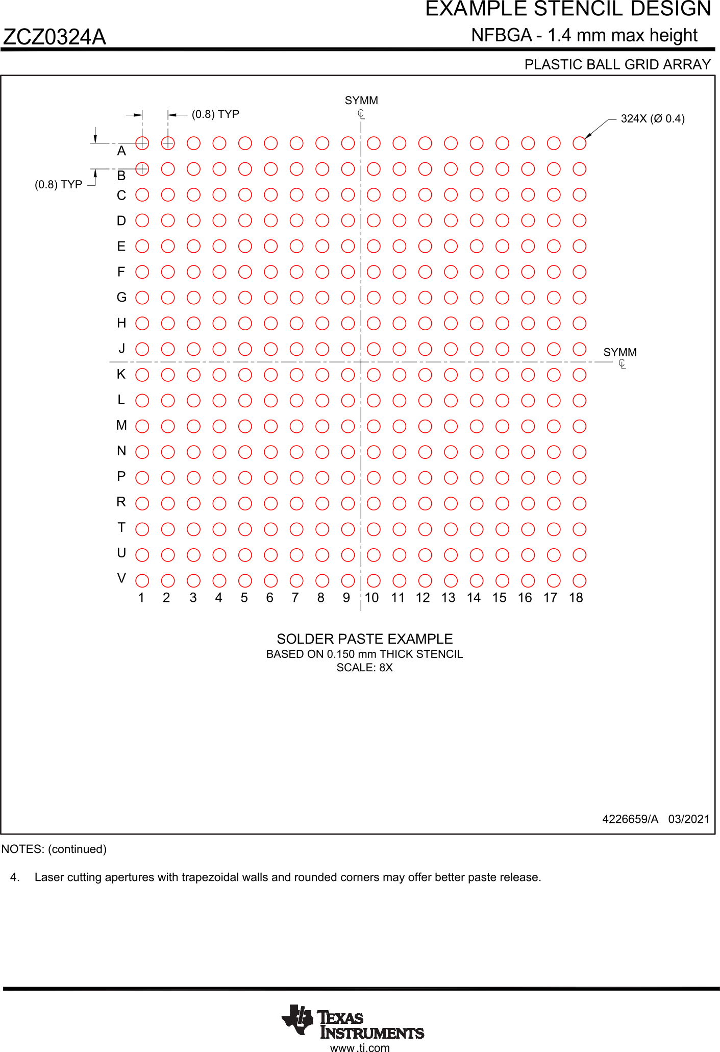
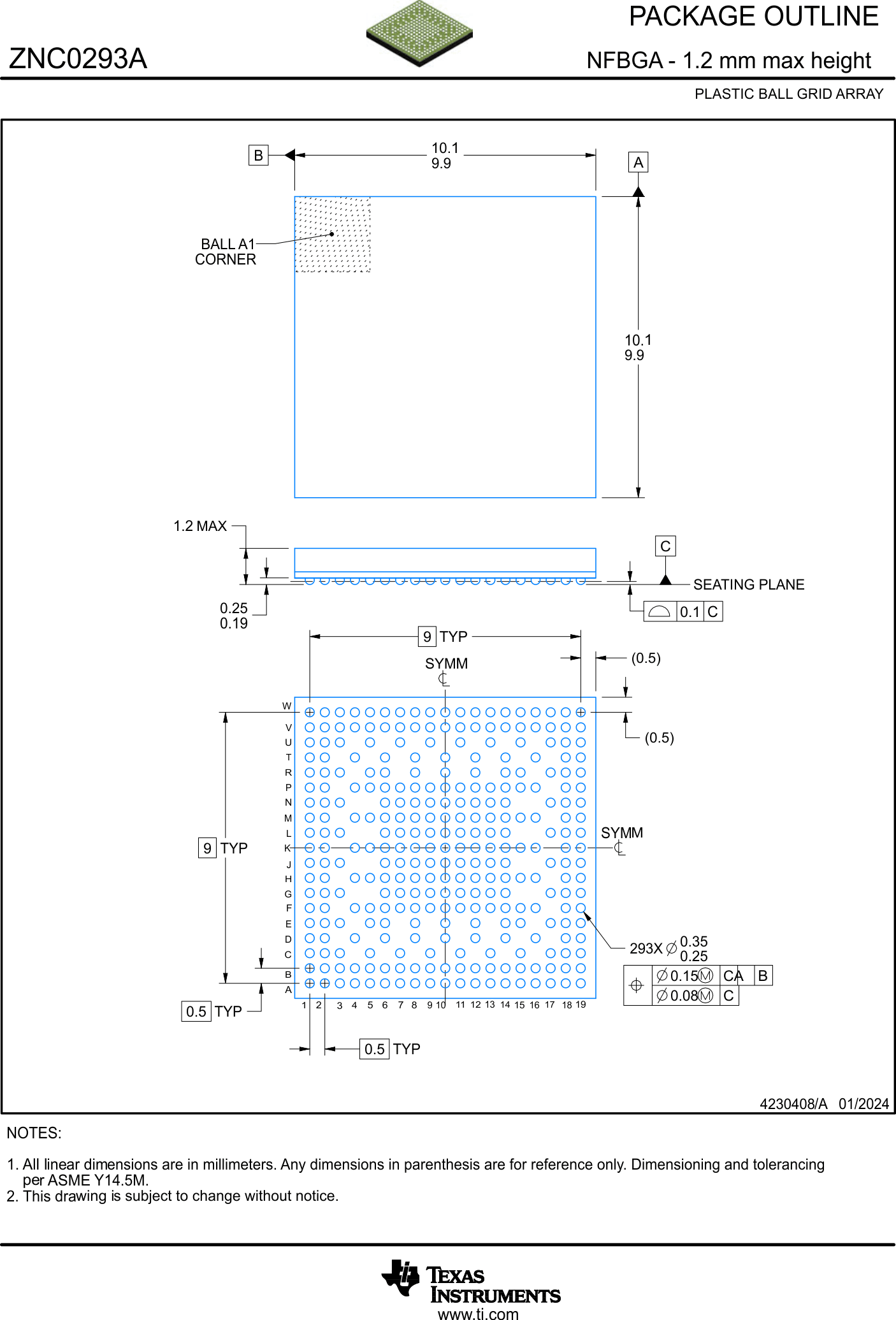
Mechanical, Packaging, and Orderable Information

The following pages include mechanical, packaging, and orderable information. This information is the most current data available for the designated devices. This data is subject to change without notice and revision of this document. For browser-based versions of this data sheet, refer to the left-hand navigation.

To learn more about TI packaging, visit the Packaging information website.
AM2612 AM2612 AM2612 AM2612 AM2612 AM2612 AM2612 AM2612 AM2612 AM2612 AM2612 AM2612