SPRUIY2 November 2024 F29H850TU , F29H859TU-Q1
- 1
- Read This First
- 1Architecture Overview
- 2Central Processing Unit (CPU)
- 3Interrupts
-
4Pipeline
- 4.1 Introduction
- 4.2 Decoupled Pipeline Phases
- 4.3 Dual Instruction Prefetch Buffers
- 4.4 Pipeline Advancement and Stalls
- 4.5 Pipeline Hazards and Protection Mechanisms
- 4.6 Register Updates and Corresponding Pipeline Phases
- 4.7 Register Reads and Writes During Normal Operation
- 4.8 D2 Read Protection
- 4.9 E1 Read Protection
- 4.10 WAW Protection
- 4.11 Protection During Interrupt
- 5Addressing Modes
- 6Safety and Security Unit (SSU)
- 7Emulation
- 8Revision History
7.3 Debug Interface
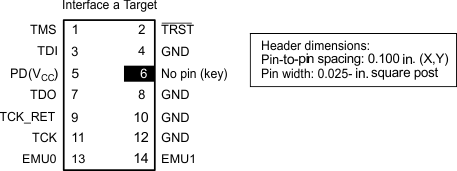
The target-level TI debug interface uses the five standard IEEE 1149.1 (JTAG) signals (TRST, TCK, TMS, TDI, and TDO) and the two TI extensions (EMU0 and EMU1). Figure 7-1 shows the 14-pin JTAG header that is used to interface the target to a scan controller, and Table 7-1 defines the pins. As listed in Table 7-1, the header requires more than the five JTAG signals and the TI extensions. The header also requires a test clock return signal (TCK_RET), the target supply (VCC), and ground (GND). TCK_RET is a test clock out of the scan controller and into the target system. The target system uses TCK_RET, if the target system does not supply a test clock (in which case TCK can not be used). In many target systems, TCK_RET is connected to TCK and used as the test clock.
 Figure 7-1 JTAG Header to Interface a
Target to the Scan Controller
Figure 7-1 JTAG Header to Interface a
Target to the Scan Controller| Signal | Description | Emulator State(1) | Target State(1) |
|---|---|---|---|
| EMU0 | Emulation pin 0 | I | I/O |
| EMU1 | Emulation pin 1 | I | I/O |
| GND | Ground | ||
| PD (VCC) | Presence detect. Indicates that the emulation cable is connected and that the target is powered up. PD must be tied to VCC in the target system. | I | O |
| TCK | Test clock. TCK is a clock source from the emulation cable pod. This signal can be used to drive the system test clock. | O | I |
| TCK_RET | Test clock return. Test clock input to the emulator. Can be a buffered or unbuffered version of TCK. | I | O |
| TDI | Test data input | O | I |
| TDO | Test data output | I | O |
| TMS | Test mode select | O | I |
| TRST(2) | Test reset | O | I |
The state of the TRST, EMU0, and EMU1 signals at device power up determines the operating mode of the device. The operating mode takes effect as soon as the device has sufficient power to operate. If the TRST signal rises, the EMU0 and EMU1 signals are sampled on the rising edge and the operating mode is latched. Some of these modes are reserved for test purposes, but those that can be of use in a target system are detailed in Table 7-2. A target system is not required to support any mode other than normal mode.
| TRST | EMU1 | EMU0 | Device Operating Mode | JTAG Cable Active? |
|---|---|---|---|---|
| Low | Low | Low | Peripheral mode. Disables the CPU and memory portions of the C29x CPU. Another processor treats the C29x CPU as a peripheral. | No |
| Low | Low | High | Reserved for testing | No |
| Low | High | Low | Wait-in-reset mode. Prolongs the device’s reset until released by external means. This allows a C29x CPU to power up in reset, provided external hardware holds EMU0 low only while power-up reset is active. | Yes |
| Low | High | High | Normal mode with emulation disabled. This is the setting that must be used on target systems when a scan controller (such as the XDS510) is not attached. TRST is pulled down and EMU1 and EMU0 pulled up within the C29x CPU; this is the default mode. | No |
| High | Low or High | Low or High | Normal mode with emulation enabled. This is the setting to use on target systems when a scan controller is attached (the scan controller controls TRST). TRST must not be high during device power-up. | Yes |