SPRUJF1 November   2024 AM2612

ADVANCE INFORMATION  

  1.   1
  2.   Description
  3.   Key Features
  4. 1LaunchPad Module Overview
    1. 2.1 Introduction
    2. 2.2 Preface: Read This First
      1. 2.2.1 If You Need Assistance
      2. 2.2.2 Important Usage Notes
    3. 2.3 Kit Contents
    4. 2.4 Device Information
      1. 2.4.1 System Architecture Overview
      2. 2.4.2 Security
      3. 2.4.3 Compliance
      4. 2.4.4 BoosterPacks
      5. 2.4.5 Component Identification
  5. 2Hardware Description
    1. 3.1  Board Setup
      1. 3.1.1 Power Requirements
        1. 3.1.1.1 Power Input Using USB Type-C Connector
        2. 3.1.1.2 Power Status LEDs
        3. 3.1.1.3 Power Tree
      2. 3.1.2 Push Buttons
      3. 3.1.3 Boot mode Selection
      4. 3.1.4 IO Expander
    2. 3.2  Functional Block Diagram
    3. 3.3  GPIO Mapping
    4. 3.4  Reset
    5. 3.5  Clock
    6. 3.6  Memory Interfaces
      1. 3.6.1 OSPI
      2. 3.6.2 Board ID EEPROM
    7. 3.7  Ethernet Interface
      1. 3.7.1 Ethernet PHY Add-on Board connector #0 - CPSW RGMII/ICSSM
      2. 3.7.2 Ethernet PHY Add-on Board connector #1 - CPSW RGMII/ICSSM
    8. 3.8  I2C
    9. 3.9  Industrial Application LEDs
    10. 3.10 SPI
    11. 3.11 UART
    12. 3.12 MCAN
    13. 3.13 FSI
    14. 3.14 JTAG
    15. 3.15 TIVA and Test Automation Pin Mapping
    16. 3.16 LIN
    17. 3.17 ADC and DAC
    18. 3.18 EQEP and SDFM
    19. 3.19 EPWM
    20. 3.20 USB
    21. 3.21 BoosterPack Headers
  6. 3Known Issues and modifications done on LP-AM261 RevE1
    1. 4.1 TA_POWERDOWNz pulled up by VSYS_TA_3V3 which is powered by VSYS_3V3
    2. 4.2 USB2.0_MUX_SEL0 pulled up by R355
    3. 4.3 MDIO and MDC of PRU0-ICSS0 needs to be routed to both Ethernet PHYs
    4. 4.4 AM261_RGMII1_RXLINK and AM261_RGMII2_RXLINK to be connected to GPIO
  7. 4Additional Information
    1.     Trademarks
    2. 5.1 Sitara MCU+ Academy
  8. 5References
    1. 6.1 Reference Documents
    2. 6.2 Other TI Components Used in This Design
    3. 6.3 Related Documentation From Texas Instruments
  9. 6Revision History

SPI

The AM261x LaunchPad maps two SPI instances (SPI0, SPI2) from the AM261x SoC to the BoosterPack Headers. Series termination resistors are placed near the SoC for each SPI clock and SPI D0 signal. There is a 2:1 mux (TS3DDR3812RUAR) that is responsible for selecting SPI0 signals for proper function. The mux is driven by an IO Expander. All SPI2 signals are directly routed to the boosterpack.
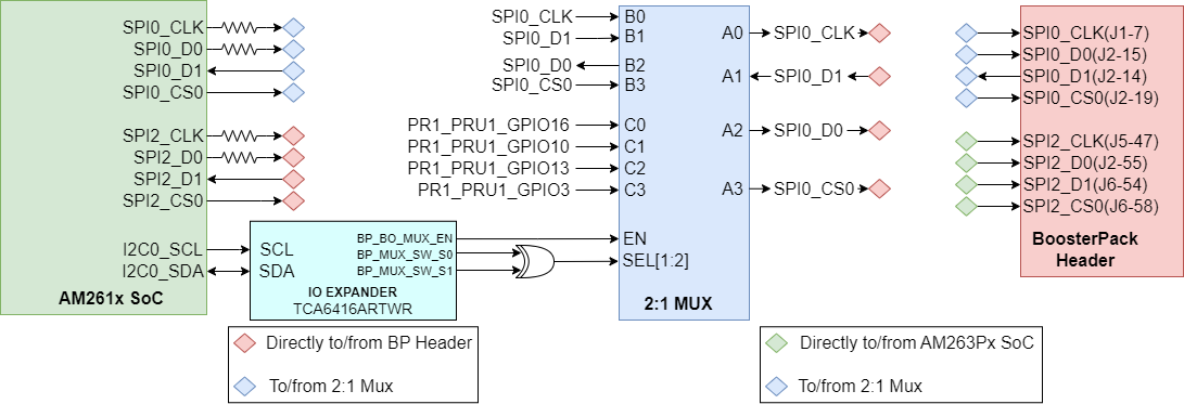
AM261x SoC SPI to BoosterPack Figure 2-18 SoC SPI to BoosterPack