-
So, What Are S-parameters Anyway? SSZT478 may 2019 ADC12DJ3200 , ADC12DJ4000RF , ADC12DJ5200RF , ADC12DL1500 , ADC12DL2500 , ADC12DL3200 , ADC12DL500 , DAC39RF10 , DAC39RF12
-
So, What Are S-parameters Anyway?
So, What Are S-parameters Anyway?
David Guidry
Modern high-speed analog-to-digital converters (ADCs) have enabled the direct sampling of radio frequency (RF) signals, which in many cases eliminates the need for mixing stages while increasing system flexibility and capability.
Traditionally, ADC signal and clock inputs have been represented by lumped element models. But for RF sampling converters, this approach is inadequate, since operating frequencies have increased to the point where a distributed representation is required.
In this three-part series, I’ll explain how to use scattering parameters, also known as S-parameters, in the design of direct RF sampling architectures.
Defining S-parameters
S-parameters provide a framework for describing networks based on the ratio of incident and reflected microwaves. This is useful for circuit design, because you can use these ratios to calculate properties such as input impedance, frequency response and isolation. It’s not necessary to know the details of the network, since it’s possible to directly measure S-parameters with a vector network analyzer (VNA).
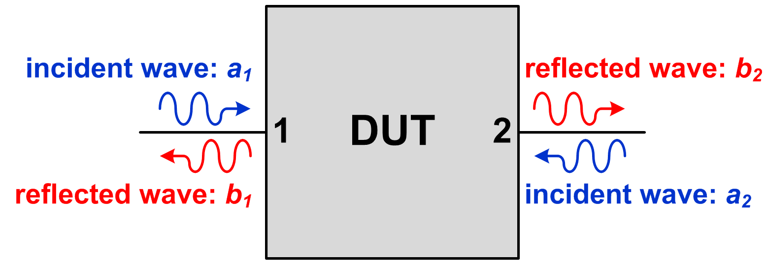
Figure 1 shows an example of a two-port network with incident wave quantities ax and reflected wave quantities bx, where x is the port. For this discussion, assume that the device under test is a linear network, and therefore superposition applies.
 Figure 1 Two-port Network Wave Quantities
Typically, the VNA stimulates one port at a time (by driving an incident wave onto that port) while measuring the reflected waves on all ports. These measured quantities are complex, since each has a corresponding amplitude and phase. The process is repeated for each port at each test frequency.
For a two-port device, you can form four meaningful ratios from the measured data. These are traditionally denoted as sij, where i is the reflected port and j is the incident port. As I mentioned, assume that only one port is stimulated at a time, so the incident wave is zero for the other ports (terminated with the system’s characteristic impedance, Z0).
Equations 1 through 4 are for the four 2-port S-parameters. S11 and S22 represent the complex impedance for ports 1 and 2, respectively. S21 represents the transfer characteristics, with port 1 as the input and port 2 as the output (S12 being the same, but with port 2 as the input and port 1 as the output).
S11 = b1/a1 while a2 = 0 (1)
S21 = b2/a1 while a2 = 0 (2)
S12 = b1/a2 while a1 = 0 (3)
S22 = b2/a2 while a1 = 0 (4)
For a unidirectional device such as an amplifier (with port 1 as the input and port 2 as the output), you can view S11 as the input impedance, S21 as the frequency response, S12 as reverse isolation and S22 as the output impedance. A data converter is also a unidirectional device, but port 2 is typically digital. This has specific implications for both measurement and interpretation.
Extending S-parameters to Multiport and Differential Devices
It is possible to extend the S-parameter framework to an arbitrary number of ports with the number of meaningful parameters equal to 2N, where N is the number of ports. Many integrated circuits have differential inputs and outputs because of increased swing and common-mode rejection. RF sampling ADCs such as TI’s ADC12DJ5200RF typically have differential RF and clock inputs. You can also further extend the S-parameter framework to support differential ports.
| Designing for demanding requirements? | |

|
Meet the requirements of tomorrow's test and measurement applications with the fastest-ever ADC. |
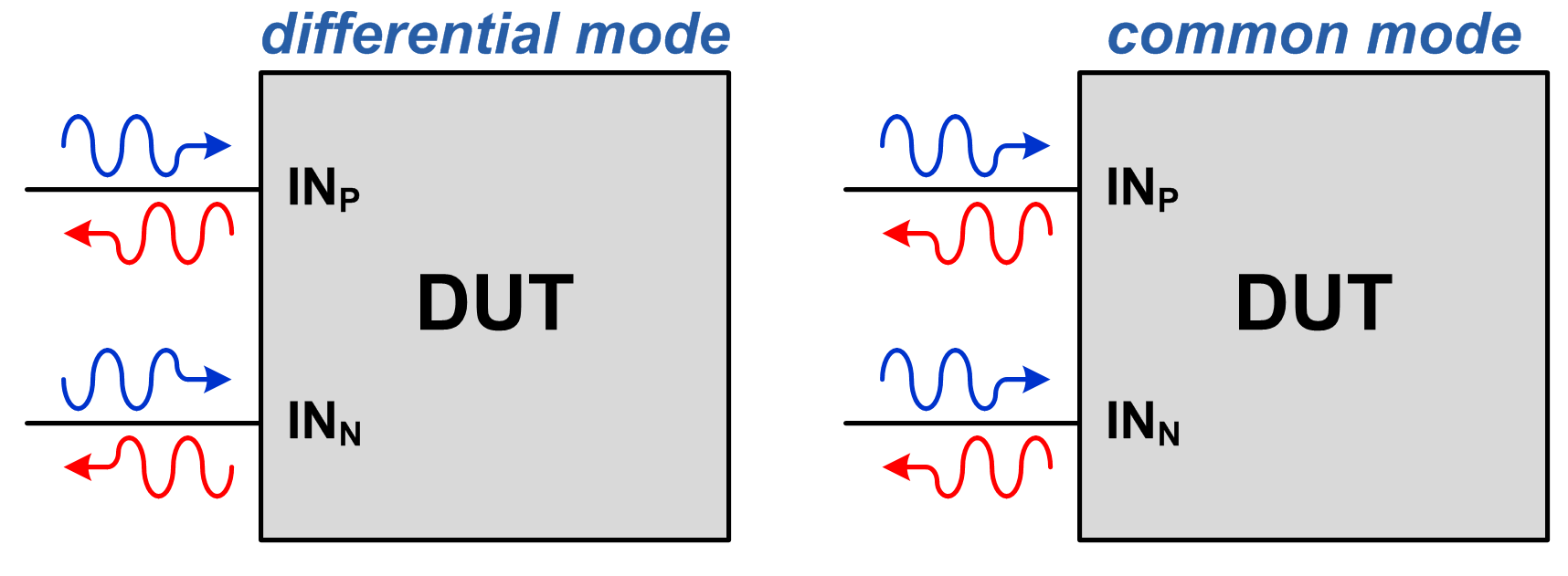
For differential ports, you must distinguish between common-mode and differential-mode waves, as shown in Figure 2. Both modes have the same incident amplitude, but differential-mode incident waves have a 180-degree phase shift whereas common-mode waves have the same phase.
 Figure 2 Differential- vs. Common-mode Waves
For linear devices without feedback between ports, superposition enables the calculation of differential and common mixed-mode S-parameters from single-ended S-parameter measurements (where only one port has an active incident wave at any given time). Modern high-performance VNAs also support the simultaneous stimulation of two ports with either differential- or common-mode waves.
Challenges When Measuring Data Converter S-parameters
The half-analog, half-digital nature of data converters poses a challenge for measuring S-parameters. VNAs cannot directly interface with the digital bus of the data converter, thus requiring ad hoc techniques to conduct the measurements.
In part 2 of this series, I will discuss the techniques developed to measure S-parameters for TI’s RF sampling data converters. Part 3 will discuss how to use S-parameters in the design of RF sampling data converter systems.
Continue reading the series in the next article, So, what's a VNA anyway?https://e2e.ti.com/blogs_/b/analogwire/archive/2019/08/23/so-what-is-the-deal-with-frequency-response
IMPORTANT NOTICE AND DISCLAIMER
TI PROVIDES TECHNICAL AND RELIABILITY DATA (INCLUDING DATASHEETS), DESIGN RESOURCES (INCLUDING REFERENCE DESIGNS), APPLICATION OR OTHER DESIGN ADVICE, WEB TOOLS, SAFETY INFORMATION, AND OTHER RESOURCES “AS IS” AND WITH ALL FAULTS, AND DISCLAIMS ALL WARRANTIES, EXPRESS AND IMPLIED, INCLUDING WITHOUT LIMITATION ANY IMPLIED WARRANTIES OF MERCHANTABILITY, FITNESS FOR A PARTICULAR PURPOSE OR NON-INFRINGEMENT OF THIRD PARTY INTELLECTUAL PROPERTY RIGHTS.
These resources are intended for skilled developers designing with TI products. You are solely responsible for (1) selecting the appropriate TI products for your application, (2) designing, validating and testing your application, and (3) ensuring your application meets applicable standards, and any other safety, security, or other requirements. These resources are subject to change without notice. TI grants you permission to use these resources only for development of an application that uses the TI products described in the resource. Other reproduction and display of these resources is prohibited. No license is granted to any other TI intellectual property right or to any third party intellectual property right. TI disclaims responsibility for, and you will fully indemnify TI and its representatives against, any claims, damages, costs, losses, and liabilities arising out of your use of these resources.
TI’s products are provided subject to TI’s Terms of Sale (www.ti.com/legal/termsofsale.html) or other applicable terms available either on ti.com or provided in conjunction with such TI products. TI’s provision of these resources does not expand or otherwise alter TI’s applicable warranties or warranty disclaimers for TI products.
Mailing Address: Texas Instruments, Post Office Box 655303, Dallas, Texas 75265
Copyright © 2023, Texas Instruments Incorporated