SSZT845 December 2017 LM27403 , LM3495
In part 1 of this series, I discussed the need for external bias and under what conditions you need to consider it. In this installment, I will look at whether you can apply external bias to any controller.
As a rule of thumb, you cannot apply external bias to controllers that have a current limit for the control field-effect transistor (FET) (also known as the high-side FET). It boils down to how the current limit is implemented.
Let’s look at a couple of examples. The first device is the LM3495, an emulated peak-current-mode buck controller. On first glance, it seems feasible that you can apply external bias on the VIN pin.
Reading through the data sheet, however, there is a section called High-Side Current Limit. A comparator monitors the voltage across the high-side FET when it is on. If the drain-to-source voltage of the high-side FET exceeds 500mV while the FET is on, the LM3495 will immediately enter hiccup mode. A 200ns blanking period after the high-side FET turns on prevents switching transient voltages from tripping the high-side current limit without cause.
Now, how is this voltage across the high-side FET actually monitored? The comparator has two inputs. The first input is the SW pin and the second input is the VIN pin. The assumption is that the drain of the high-side FET and VIN pin are always at one potential.
This configuration saves a pin, but it makes the external bias problematic. Let’s say that you apply 5V as the external bias to the VIN pin. The input voltage is 3.3V, applied to the drain of the high-side FET. This causes a 1.7V difference across the comparator looking for 500mV, so the controller enters hiccup mode.
The next device example is the LM27403. Looking through the data sheet, there is no current sensing for the high-side FET. Thus, you can use this device for supplying external bias to the VDD pin in low VIN applications.
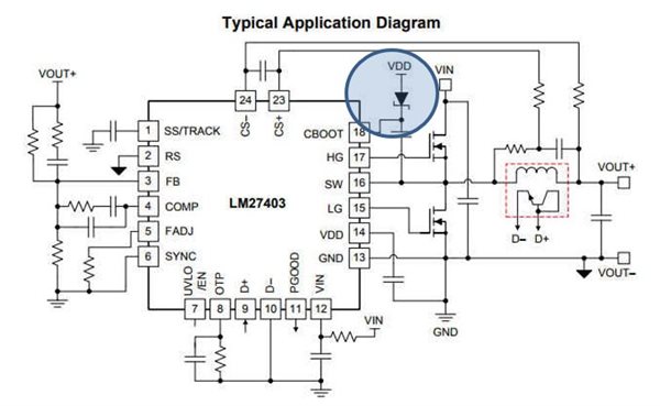
How did I know to apply the external bias to the VDD pin? Let’s look at the block diagram of the device shown in Figure 1. Take note of the supply voltage shown for the low-side FET drive circuit; in this case, it’s VDD. If you look at the application circuit in Figure 2 you’ll see where CBOOT is connected through the diode. For the LM27403, it is also VDD. Thus, you can determine that VDD is the right pin with which to apply the external bias.
 Figure 1 Block Diagram Showing
VDD
 Figure 2 Application Circuit
Showing VDD
Figure 2 Application Circuit
Showing VDDNow the question is how to determine what value of voltage is OK to apply at the VDD pin. For this, you need to refer to the absolute maximum ratings of the VDD pin and make sure that the external bias applied does not violate this rating. Looking at the LM2403 data sheet, the absolute maximum for VDD is 6V and the recommended operating maximum is 5.5V.
5V is a common rail on boards and would serve as an appropriate bias voltage. The bias voltage needs to be a regulated voltage in order to not violate the absolute maximum ratings of the VDD pin.
In part 3 of this series, I will explore ways to generate your own external bias voltage (in the event that 5V rails are not available) by using charge-pump schemes from the very supply to which you need to supply the external bias.