SSZTA08 July 2017 TPS65642
If you ever had the pleasure to design the bias supply for a Thin Film Transistor Liquid Crystal Display (TFTLCD) module and you used the appropriate part from TI then you may have run into the temperature compensation function. This blog will handle the background on why a Liquid Crystal Display (LCD) needs temperature compensation and how it is implemented in TI’s LCD Bias IC’s.
Before I evaluate the temperature effect let’s touch quickly on how the LCD actually shows a picture.
A LCD is built up like a sandwich. The actual liquid crystal is covered with two plates of glass, the upper side coated with the color filter and polarizer, the lower plate deposited with TFTs to address the pixels and a polarizer as well. The actual light is coming from the backlight at the bottom. Since the 70's we know that the liquid crystal twists if an electric field is applied. Dependent on the voltage level the crystal aligns such that it either blocks or passes the backlight.
 Figure 1 LCD Profile
Each pixel consists of three sub-pixels with different color filter (Red, Green and Blue). Each of the sub-pixels is controlled by a TFT, see the structure and equivalent circuit in Figure 2.
 Figure 2 Unit Pixel Structure +
Equivalent Circuit
Figure 2 Unit Pixel Structure +
Equivalent CircuitThe actual picture information (data line) decides the level of voltage across the crystal (equivalent to the storage capacitor Cs and the liquid-crystal capacitor Clc).
The time frame to activate the pixel is set by the voltage at the gate of the TFT (gate line).
Now, a positive voltage (also commonly called VGH or VON) is applied to the gate and the TFT (here N-channel) turns on. Clc and Cs charge up to the voltage applied to the data line. The maximum voltage on the data line is called AVDD or VS. This is transferred to the pixel electrode and becomes visible. Vice versa, a negative voltage (also called VGL or VOFF) turns off the transistor, the intrinsic capacitors of the LC discharge and the data voltage will not be transferred.
On a FHD / 60 Hz display for example each cycle (turn-on, turn-off) needs to happen within approx. 10 µs. *FHD = 60 Hz / (1920 x 1080 pixel x 3 (RGB)) = 9.6 µs
Temperature has two big impacts on the performance of the LCD.
The first is that the actual LC fluid changes its viscosity over temperature. At cold temperatures, the viscosity of the LC fluid decreases and this increases the response time of the crystal to the applied voltages. This effect comes with the LCD technology and can only be tailored accordingly by the panel supplier.
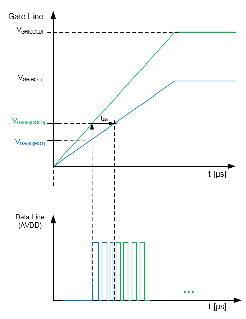
The second effect is that the operating conditions of the TFTs are changing. Studies have shown that the threshold voltage of an amorphous silicon (a-Si) TFT increases as the temperature decreases. Figure 4 shows how this can affect the on-time transition (VGH). In a warm environment (25°C to 80°) the thresholds are quite low, the transistor switches fast enough to make sure that the picture information (Data Line) is put through to the pixel and transfers the correct light intensity.
However, cold temperatures cause the switch to turn on slower. This steals time (tΔth) to put through the picture information, see figure below. Less light comes through the filter glass and the contrast gets lower. Visible results are flickering and/or image sticking of the display.
 Figure 3 Temperature Behavior
TFT
Figure 3 Temperature Behavior
TFTIn order to maintain the correct throughput of the picture information at a lower temperature, the turn-on voltage VGH needs to be increased. This is where the temperature compensation kicks in. From the experience with panel suppliers, it is an empirical approach to set the hot and cold voltage requirements.
How is the temperature compensation implemented?
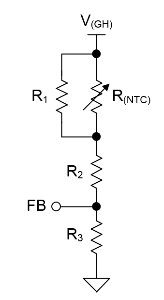
If you need to build up your own compensation network, the simplest solution to adjust a temperature dependent voltage is the circuit as below:
 Figure 4 Simple Compensation
Network
Figure 4 Simple Compensation
NetworkThe most common way to measure the ambient temperature is to use a negative temperature coefficient thermistor and place it on the LCD control PCB where it represents the ambient temperature the best. As described the LCD module should specify the normal operating turn-on voltage VGH and the temperature coefficient requirements. With this, you can apply the thermistor in parallel to the upper resistor of the feedback network of the voltage regulator. This solution has the disadvantage that the voltage cannot be monitored and cannot be covered by a maximum and a minimum value. Many of today’s LCD bias solutions are programmable with an I2C compatible interface and feature the temperature compensation with an NTC thermistor network.
Let’s take the TPS65642 for example. Figure 5 shows the block diagram of how the gate-charge voltage rail VGH can be compensated in this part.
 Figure 5 Temperature Compensation
Network TPS65642
Figure 5 Temperature Compensation
Network TPS65642The external resistive voltage divider RT1, RT2 and RNTC sinked by a fixed current source ISET set the initial voltage and the adjustment range from TCOLD to THOT. Use this calculation sheet to get the maths.
Once the temperature corners are set on hardware the device needs to be programmed with the voltage corners VGH(HOT) and VGH(COLD). The value for VGH(COLD) , usually the upper value is set in DAC1 (25 V to 40 V scaled down to 0.893 V to 1.429 V) and the value for VGH(HOT) , usually the lower value is set in DAC2 (16 V to 30 V scaled down to 0.571 V to 1.107 V).
The resistance of the NTC network increases with decreasing temperature. This means that the voltage on TCOMP increases with decreasing temperature. If the voltage exceeds the lower corner, Q1 turns on and sets the signal for the PWM controller to increase VGH. The resistive dividers R2/R1 set the transition slope and R3/R4 is the feedback divider for VGH.
It is also possible to set a positive temperature slope. For this, you either use a PTC thermistor instead or place the NTC thermistor parallel to the upper resistor RT1.
If you have experienced your panel having different requirements regarding temperature behavior just leave your comment below, we are interested to know.