How to Optimize Differential Amplifier Noise
Signal gain and noise gain are both important to amplifier circuit design. Signal gain is obviously important because you want to have accurate control of your signal amplitude. Noise gain is also important, even though it does not directly impact signal amplitude, because it impacts amplifier stability and loop gain, both of which have an impact on signal quality. Thus, it’s important to be able to calculate both noise gain and signal gain for a particular circuit. Once you have these numbers, you can use the datasheet guidelines to optimize your circuit.
Let’s quickly review signal gain with
fully differential amplifiers, both inputs are inverting inputs; there is no
noninverting input, so your signal gain is  . When you build the board, you physically solder RF onto the
board, so you know the value of RF – or do you? Depending on the particular
amplifier and board design, you may need to consider extra resistance. TI’s LMH5401 fully differential amplifier has an extra 25Ω on
chip between the amplifier output and the feedback connection pins on the amplifier
package. Because this amplifier is only 3mm by 3mm, and because the feedback
connection pins are directly adjacent to the amplifier input pins, any measurable
board resistance is not likely. You should, however, consider any board traces
longer than 1cm possible sources of extra resistance. So if you’re using the LMH5401, you’ll need to add onboard feedback resistance
to the on-chip resistance.
. When you build the board, you physically solder RF onto the
board, so you know the value of RF – or do you? Depending on the particular
amplifier and board design, you may need to consider extra resistance. TI’s LMH5401 fully differential amplifier has an extra 25Ω on
chip between the amplifier output and the feedback connection pins on the amplifier
package. Because this amplifier is only 3mm by 3mm, and because the feedback
connection pins are directly adjacent to the amplifier input pins, any measurable
board resistance is not likely. You should, however, consider any board traces
longer than 1cm possible sources of extra resistance. So if you’re using the LMH5401, you’ll need to add onboard feedback resistance
to the on-chip resistance.
 Figure 1 Circuit with a Signal Gain of
1 and Noise Gain of 2
Figure 1 Circuit with a Signal Gain of
1 and Noise Gain of 2As shown in Figure 1, the signal gain is equal to 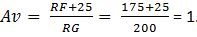 But when I run a TINA-TITM simulation, I don't get the
expected 0dB of gain. The LMH5401 has two 10Ω resistors, one on each output pin.
Adding those resistors into the equation gives you
But when I run a TINA-TITM simulation, I don't get the
expected 0dB of gain. The LMH5401 has two 10Ω resistors, one on each output pin.
Adding those resistors into the equation gives you 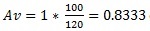 or -1.6 dB, which does match the TINA-TI simulation.
Something else also shows up on the
TINA-TI simulation: gain peaking on the frequency response, indicating possible
instability. The datasheet states that, "For the LMH5401, NG > 3 creates a stable circuit independent
of how the signal gain is set." What's the noise gain of the circuit in Figure 1? In the circuit shown in Figure 1, noise gain:  . Thus, this circuit is not stable according to the datasheet. Note that the resistive loss on the output
resistors is not included in noise gain, even though they do contribute to loss in
the signal path.
. Thus, this circuit is not stable according to the datasheet. Note that the resistive loss on the output
resistors is not included in noise gain, even though they do contribute to loss in
the signal path.
 Figure 2 Frequency Response for the
Circuit Shown in Figure 1
Figure 2 Frequency Response for the
Circuit Shown in Figure 1Just for curiosity's sake, let's run a TINA-TI simulation and see what the noise looks like.
 Figure 3 Noise Response for the Circuit
Shown in Figure 1
Figure 3 Noise Response for the Circuit
Shown in Figure 1Notice the peak in noise amplitude in Figure 3. This instability also shows up in the noise response. The datasheet states that the input-voltage noise for the LMH5401 is 1.25nV/rtHz. If the noise gain is indeed 2, you would expect to see the amplifier output noise to be approximately 2.5nV/rtHz. The results are very close. The extra noise in the simulation is due to current noise as well as the resistors in the circuit. So the noise gain is indeed 2.
I should also point out that the extra high-frequency noise (centered at 4GHz) is not due to noise gain but to the loss of phase margin. As phase margin decreases, the feedback circuit begins to dramatically add gain as the feedback transitions from negative feedback to positive feedback.
The datasheet gives you the option to increase noise gain (and not signal gain) to make the amplifier stable. Figure 4 shows one simple way to accomplish this.
 Figure 4 Circuit with a Signal Gain of
1 and Noise Gain of 6
Figure 4 Circuit with a Signal Gain of
1 and Noise Gain of 6In Figure 1, noise gain was  . While Figure 4 has only one more component, it is easier to calculate the noise
gain if you imagine that R6 is two resistors of 50Ω each, connected to an ideal
(noiseless) voltage source of 0V. In this case, half of R6 is in parallel with RG,
so the noise gain is now
. While Figure 4 has only one more component, it is easier to calculate the noise
gain if you imagine that R6 is two resistors of 50Ω each, connected to an ideal
(noiseless) voltage source of 0V. In this case, half of R6 is in parallel with RG,
so the noise gain is now 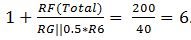 . A noise gain of 5 works, but the
datasheet specifies a noise gain of 3 as the minimum
required. In order to reduce the amount of output noise, let’s go with the datasheet’s minimum noise gain of 3. This requires an R6
value of
. A noise gain of 5 works, but the
datasheet specifies a noise gain of 3 as the minimum
required. In order to reduce the amount of output noise, let’s go with the datasheet’s minimum noise gain of 3. This requires an R6
value of 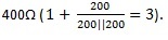 .
.
 Figure 5 Noise Response for the Circuit
Shown in Figure 4 With a Noise Gain of 6
Figure 5 Noise Response for the Circuit
Shown in Figure 4 With a Noise Gain of 6 Figure 6 Noise Response for the Circuit
with a Noise Gain of 3
Figure 6 Noise Response for the Circuit
with a Noise Gain of 3The plot in Figure 5 shows that the noise gain has indeed increased (it's equal to 6V/V) and there is no peaking in the noise response. Figure 6 shows that the amplifier is also stable at a noise gain of 3V/V, and the noise level is less than that shown in Figure 5, except at very high frequencies.
I hope I've shown how you can manipulate signal gain and noise gain independently to optimize circuit performance. In what applications could you apply these methods?
Additional Resources
- Download the LMH5401 datasheet.
- Check out my other high-speed amplifier blog posts.
- Search TI high-speed op amps and find technical resources.