SSZTCV2 August 2017 LMG3522R030 , UCD3138
Microprocessors and application-specific integrated circuits (ASICs) require low-voltage, high-current power supplies. These supplies usually have very strict requirements on output-voltage deviations, especially to load transient events. Testing these supplies can pose a challenge for designers, and it may be difficult to confirm compliance with the specifications.
In Power Tip 63, Robert Kollman covered some of the issues associated with load transient testing. Here, I will cover additional details as well as methods that you can use to simplify testing of these difficult conditions.
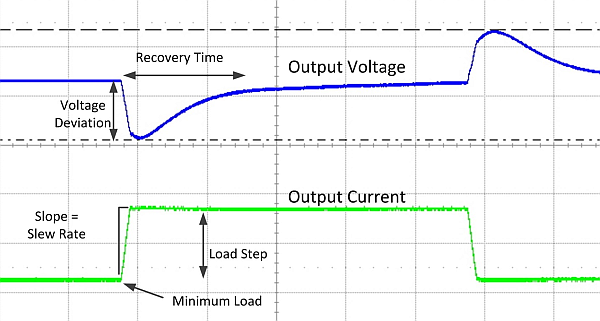
First, you need to understand all of the transient specifications in order to properly design the supply, while also understanding how they apply to the testing. Typical transient specifications include:
- The size of the load step in amperes or given as a percentage of the full load.
- The minimum load during a transient event (sometimes zero).
- The slew rate of the load step, usually in amperes per microsecond.
- The maximum voltage deviation allowed on both edges of the step.
- The expected recovery time.
Figure 1 shows an example of how these specifications are usually defined.
 Figure 1 Graphical description of a load transient measurement
Once you understand all of the specifications, you can attempt to design the supply to meet the requirements. Testing said requirements then becomes the challenge, however. It is not unusual to see requirements for an output voltage of 1V, a load step of 100A and a slew rate of 1,000A/µs. The limiting factor in most testing situations is the inductance between the power supply under test and the load. In a real system, the power supply is often right next to the load it is powering; thus the parasitic inductance is minimized.
You can use a number of methods to test the load transient response for a given power supply; each has its pros and cons. Here, I’ll compare the following options: an external electronic load, an external transient board, a “field-effect transistor (FET) slammer,” an onboard transient generator and a socket-based transient tester.
The external electronic load is probably the most common method for testing transient response – and the most convenient. Most loads have modes that enable you to easily set the current levels and transition times. The main drawback is limited slew rate, either caused by external wiring or limitations of the actual load.
An external transient board can usually achieve better results in terms of slew rate, but at the cost of flexibility. Depending on the design, the load transient board may be limited in maximum current, thermal dissipation or slew rate. Because the transient board is connected externally, wiring is often the slew-rate-limiting bottleneck. Also, you need to adjust or configure the board for each power supply that you test.
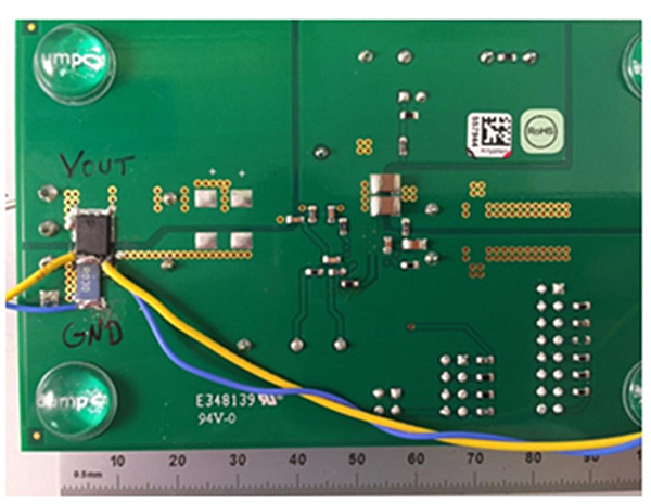
A FET slammer is a quick and crude method for getting high-speed transient results. You connect a metal-oxide semiconductor field-effect transistor (MOSFET) from drain to source through a resistor or directly across the output of the power supply; a function generator controls the gate. Because there is minimal external wiring, there’s a major reduction in parasitic inductance.
While this method can usually generate a high slew rate, the control and repeatability of the testing may be difficult. You may also have to modify the printed circuit board (PCB) (Figure 2). Another issue with this method is that measuring the actual load step current is difficult and can be inaccurate.
 Figure 2 Example of a PCB with a FET
slammer
Figure 2 Example of a PCB with a FET
slammerOnboard transient generators can be very helpful when trying to test the performance of high-current high-speed transients. You can design the circuit for the exact load transient specification. The main drawbacks are extra cost and space taken by the components. In addition, the flexibility to take multiple different measurements might be difficult or time-consuming.
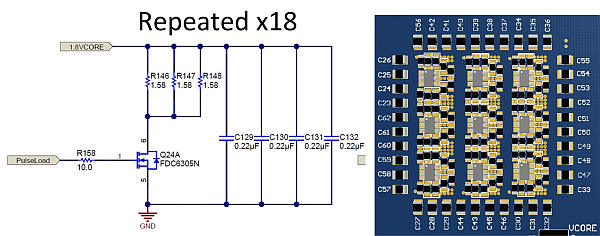
The design of an onboard transient generator can be quite complex as well. It can be as simple as a resistor and FET controlled by a 555 timer or as complicated as something like what’s shown in Figure 3. The more complex design uses multiple stages and smaller, faster-switching FETs. This type of design can achieve slew rates of 1,000A/µs.
 Figure 3 A more complex version of an onboard transient generator
The final option is to use a processor socket and a specialized transient tester tool. This option is the most expensive route, as the tool itself can be expensive and the PCBs become much more costly. However, you may achieve the most accurate results for a given set of processor requirements. The processor or ASIC manufacturer often develops these tools, so they are built specifically to deliver the right test conditions.
Table 1 summarizes the transient testing options.
| Method | Pros | Cons |
|---|---|---|
| External electronic load | Simple, flexible, possibly no extra cost | Limited slew rate due to external connections |
| External transient board | Simple, low cost | Needs to be modified for each test; limited slew rate due to external connections |
| FET slammer | Low cost, fast slew rates | Requires a fancy function generator; measuring the actual current can be difficult and inaccurate; possibly hard to control |
| Onboard transient generator | Very fast slew rates; designed specifically for the supply under test | Each different test condition requires modifications to the board; takes up extra space on the PCB; could add cost; difficult to measure current |
| Socket-based transient tester | Very specific testing for exact compliance; generally controlled through software to make testing easy | Very expensive; difficult PCB layout to accommodate socket; PCBs can be very expensive because of layer count and socket placement |
Testing for load transients is a very important part of power-supply design and compliance. Parasitic inductance in test fixtures can negatively impact your ability to achieve the desired slew rates. Using the methods I’ve described here, I hope you can avoid this problem.
To learn more about transient loads, read the Power House blog: Power Tips: A Simple Circuit Yields Fast, Controllable Transient Loads.
For more Power Tips, check out TI’s Power Tips blog series.
Also see:
- Testing a power supply
- Load-transient-response testing for voltage regulators
- Power Tip 63: Testing High-di/dt Power Supplies
- Power Tips #78: Synchronous rectifiers improve cross-regulation in flyback power supplies
- Power driver design handles difficult loads, helps characterize PSUs
- Power transient buffer enables IC & circuit testing
- Transient load gives power systems a workout
Previously published on EDN.com.