SSZTCV4 February 2024 LMG3526R030 , TMS320F280049C , UCC27517
The need for cost-effective solutions to improve power factor correction (PFC) at light loads and with peak efficiency while shrinking passive components is becoming difficult with conventional continuous conduction mode (CCM) control. Engineers are conducting significant research into complex multimode solutions to address these concerns [1], [2], and these approaches are attractive in that they enable you to shrink the size of the inductor while simultaneously improving efficiency with soft switching at lighter loads.
But in this power tip, I will present a new approach to achieving high efficiency and low total harmonic distortion (THD) that does not require the use of a complex multimode control algorithm and achieves zero switching losses under all operating conditions. This approach uses a high-performance gallium-nitride (GaN) switch with an integrated flag that indicates whether the switch turns on with zero voltage switching (ZVS). This approach enables high-efficiency ZVS under all operating conditions while simultaneously forcing the THD very low.
Topology
The topology used for this system is the integrated triangular current mode (iTCM) totem-pole PFC [3]. For high-power and high-efficiency systems, the totem-pole PFC offers a distinct advantage for conduction losses. The TCM version of this topology enforces ZVS by making sure that the inductor current always goes sufficiently negative before the switch turns on [4]. Figure 1 illustrates the iTCM version of totem-pole PFC.
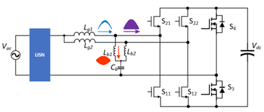 Figure 1 The iTCM topology, showing AC line frequency current envelopes.
The difference between the TCM converter and the iTCM converter is the presence of Lb1, Lb2 and Cb. During normal operation, the voltage across Cb is equal to the input voltage Vac. Two phases operating 180 degrees out of phase take advantage of ripple current cancellation and reduce the root-mean-square current stress in Cb. Lb1 and Lb2 are sized to only process the high-frequency AC ripple current necessary for TCM operation. This removes the DC bias required for the inductor used in TCM, as defined in [4]. Ferrite cores for Lb1 and Lb2 help ensure low losses in the presence of the high flux swings necessary for ZVS. Lg1 and Lg2 are larger in value (as much as 10 times larger) than Lb1 and Lb2, which prevents most of the high-frequency current from flowing into the input source and subsequently reduces electromagnetic interference (EMI). In addition, the reduced ripple current in Lg1 and Lg2 enables the possible use of lower-cost core materials. Figure 1 also illustrates the ripple current envelopes for several key branches.
Control
Control is facilitated by the Texas Instruments (TI) TMS320F280049C microcontroller and LMG3526R030 GaN field-effect transistors (FETs). These FETs have an integrated zero-voltage-detection (ZVD) signal that is asserted anytime the switch turns on with ZVS. The microcontroller uses the ZVD information to adjust the switch timing parameters to turn the switch on with just enough current to achieve ZVS. For simplicity, Figure 2 illustrates a one-phase iTCM PFC converter. Table 1 defines the key variables used in this figure. The microcontroller uses an algorithm that solves the exact set of differential equations for the system. These equations use conditions that enforce ZVS on both switches and force the current to be equal to the current command. The equations are accurate, provided that the system is operating with the right amount of ZVS for both switches. When operating correctly, the algorithm yields the timing parameters for 0% THD and an optimal amount of ZVS. To facilitate the ZVS condition, each switch (S1 and S2) reports their respective ZVS turnon status on a cycle-by-cycle basis back to the microcontroller. In Figure 2, Vhs,zvd and Vls,zvd denote the ZVD reporting.
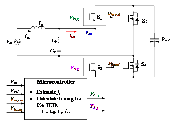 Figure 2 A single-phase iTCM schematic with control signals.

|
Figure 3 illustrates the ZVD timing adjustment process. During every switching cycle, the microcontroller calculates the switch timing parameters (ton, toff, trp, and trv) based on the ZVD signal’s cumulative history. Figure 3b shows the system operating at the ideal frequency. By ideal, I mean that the THD is 0%, and you have the perfect amount of ZVS for the high- and low-side FETs. Figure 3a shows what happens when the operating frequency is 50 kHz lower than the ideal. Notice that the high-side FET loses ZVS (as indicated by the loss of the high-side ZVD signal), while the low-side FET has more negative current than is necessary to achieve ZVS. The result is a loss of efficiency and a distorted power factor. Figure 3c occurs when the operating frequency is 50 kHz higher than the ideal. In this case, the high-side FET has ZVS but the low-side FET loses ZVS. Again, there is a clear loss of efficiency and distortion.
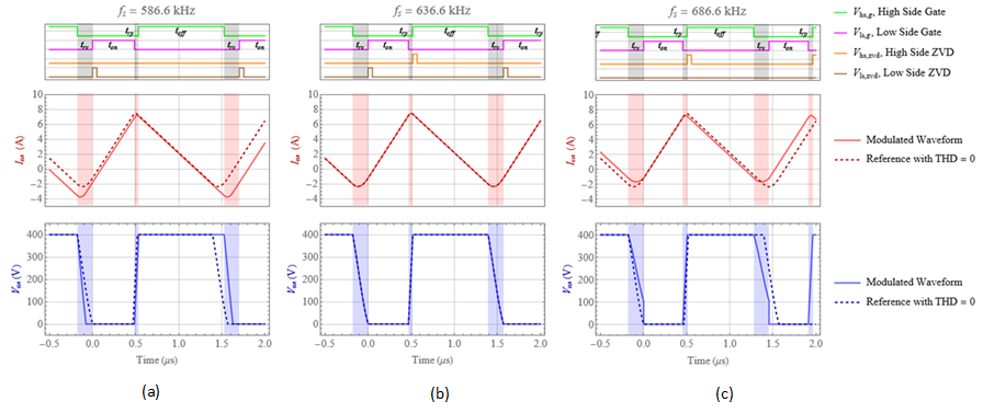 Figure 3 ZVD behavior with low fs (a); ideal fs (b); and high fs (c).
Based on the presence or absence of the ZVD signal, the controller can increase or decrease the frequency to push the system to the optimum operating point. In this way, the control effort acts like an integrator that attempts to find the best operating frequency. The optimum will occur when the system is hovering right on the threshold of just barely getting ZVS every cycle.
Prototype performance
Figure 4 shows a prototype built with the topology and algorithm I’ve discussed so far.
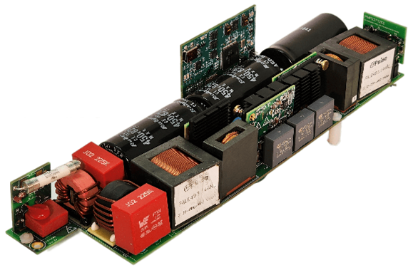 Figure 4 A 400-V, 5-kW prototype with a
power density of 120 W/in3.
Figure 4 A 400-V, 5-kW prototype with a
power density of 120 W/in3.Table 2 summarizes the specifications and important component values for the prototype.

|
Figure 5 shows the prototype’s measurement nodes and Figure 6 illustrates the system waveforms of the prototype operating under full power (5 kW). The switch-node currents, IL,A and IL,B, are the sum of the current in Lg and Lb for their respective branch. The zoom section of the plot shows the waveform detail during the positive half cycle. The current waveforms have an ideal triangular shape, with just enough negative current to achieve ZVS as demonstrated by switch-node voltages VA and VB. Furthermore, the sinusoidal envelope of the current waveform suggests a low THD.
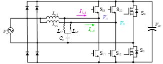 Figure 5 Prototype measurement nodes
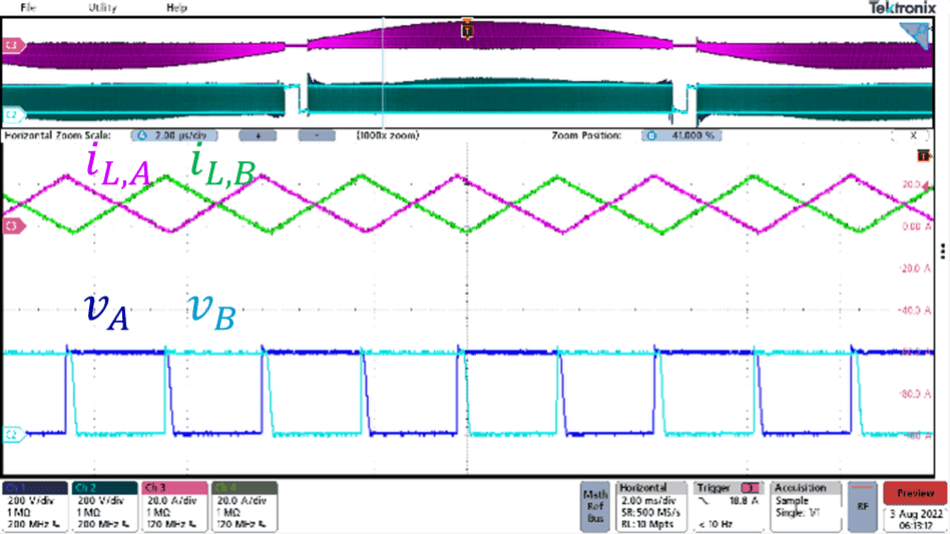 Figure 6 System waveforms of the prototype operating under full power (Vin = Vout/2, load = 5 kW, Vin = 230 Vac, Vout = 400 V).
Figure 7 shows the measured efficiency and THD across the load range. The efficiency peaks above 99% and is above 98.5% for almost the entire load range. The THD has a maximum of 10% and is below 5% for most of the load range. In order to optimize performance, the unit phase sheds or adds phases at approximately 2 kW.
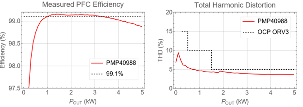 Figure 7 The prototype efficiency and THD across the load range.
Achieving a high efficiency and low THD for a totem-pole PFC
You can use the ZVD signal to control the operating frequency of a totem-pole PFC converter to achieve high efficiency and low THD. For more information about this approach, as well as a simulation model for the system, see the Variable-Frequency, ZVS, 5-kW, GaN-Based, Two-Phase Totem-Pole PFC Reference Design.
Related Content
- Power Tips #114: A potential firmware mistake may lead to control instability
- Power Tips #113: Two simple isolated power options for 8 W or less
- Power Tips #112: Onboard fixtures for fault testing
- Power Tips #111: Why current sensing is a must in collaborative, mobile robots
- PFC totem pole architecture and GaN combine for high power and efficiency
- GaN transistors for efficient power conversion: buck converters
References
- Fernandes, Ryan, and Olivier Trescases. “A Multimode 1-MHz PFC Front End with Digital Peak Current Modulation.” Published in IEEE Transactions on Power Electronics 31, no. 8 (August 2016): pp. 5694-5708. doi: 10.1109/TPEL.2015.2499194.
- Lim, Shu Fan, and Ashwin M. Khambadkone. “A Multimode Digital Control Scheme for Boost PFC with Higher Efficiency and Power Factor at Light Load.” Published in 2012 Twenty-Seventh Annual IEEE Applied Power Electronics Conference and Exposition (APEC), Feb. 5-9, 2012, pp. 291-298. doi: 10.1109/APEC.2012.6165833.
- Rothmund, Daniel, Dominik Bortis, Jonas Huber, Davide Biadene, and Johann W. Kolar. “10kV SiC-Based Bidirectional Soft-Switching Single-Phase AC/DC Converter Concept for Medium-Voltage Solid-State Transformers.” Published in 2017 IEEE 8th International Symposium on Power Electronics for Distributed Generation Systems (PEDG), April 17-20, 2017, pp. 1-8. doi: 10.1109/PEDG.2017.7972488.
- Liu, Zhengyang. 2017. “Characterization and Application of Wide-Band-Gap Devices for High Frequency Power Conversion.” Ph.D. dissertation, Virginia Polytechnic Institute and State University. http://hdl.handle.net/10919/77959.
Previously published on EDN.com.