SWRA465A August 2014 – July 2015 CC2530 , CC2530 , CC2530-RF4CE , CC2530-RF4CE , CC2592 , CC2592
- Using CC2592 Front End With CC2530
- A Marker - Delta Method
- Revision History
8 Controlling the CC2592
There are three digital control pins (PA_EN, LNA_EN and HGM) on the CC2592 that control the state of the chip. Table 10 shows the control logic when connecting the CC2592 to a CC2530 device.
Table 10. Control Logic for Connecting the CC2592 to a CC2530 Device
| PA_EN | LNA_EN | HGM | Mode of Operation |
|---|---|---|---|
| 0 | 0 | X | Power Down |
| X | 1 | 0 | RX Low Gain Mode |
| X | 1 | 1 | RX High Gain Mode |
| 1 | 0 | X | TX |
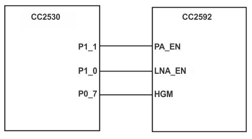
The SimpleLink™ ZigBee® Network Range Extender Reference Design[3] uses three of the CC2530 GPIO pins on the CC2530 to control the CC2592. The I/O pins used are shown in Figure 12. PA_EN and LNA_EN must be controlled by RF observation signals as shown in Figure 12, whereas, the HGM pin can be controlled by any GPIO or alternatively tied to VDD or GND.
 Figure 12. CC2530-CC2592 Interconnect
 When using the CC2592 with the CC2530, the RF observation registers must be set according to Table 11. This enables the RF core of CC2530 to control the CC2592 through P1. If required, other P1 pins can be used, see the CC2538 System-on-Chip Solution for 2.4-GHz IEEE 802.15.4 and ZigBee®/ZigBee IP® Applications User's Guide (SWRU319) for details.
Table 11. CC2530 Registers for CC2592 Control
| CC2530 REGISTER | RECCOMMENDED VALUE |
|---|---|
| AGCCTRL1 | 0x15 |
| FSCAL1 | 0x00 |
| RFC_OBS_CTRL0 | 0x68 |
| RFC_OBS_CTRL1 | 0x6A |
| TXPOWER | See Table 6 |
| OBSSEL1 | 0xFB |
| OBSSEL0 | 0xFC |
| P0DIR | 0x80 |