SWRA640H December   2018  – May 2024 CC1310 , CC1312R , CC1314R10 , CC1350 , CC1352P , CC1352R , CC1354P10 , CC1354R10 , CC2620 , CC2630 , CC2640 , CC2640R2F , CC2640R2F-Q1 , CC2642R , CC2642R-Q1 , CC2650 , CC2652P , CC2652R , CC2652R7 , CC2652RB , CC2652RSIP , CC2674P10 , CC2674R10


  1.   1
  2.   Abstract
  3.   Trademarks
  4. Reference Design
    1. 1.1 Sub-1GHz LaunchPads
      1. 1.1.1 LAUNCHXL-CC1310
      2. 1.1.2 LAUNCHXL-CC1312R
    2. 1.2 2.4GHz LaunchPads
      1. 1.2.1 LAUNCHXL-CC2640R2
      2. 1.2.2 LAUNCHXL-CC26x2R
      3. 1.2.3 LP-CC26x1
    3. 1.3 Dual-Band LaunchPads
      1. 1.3.1 LAUNCHXL-CC1350EU/US
      2. 1.3.2 LAUNCHXL-CC1350-4
      3. 1.3.3 LAUNCHXL-CC1352R
      4. 1.3.4 LAUNCHXL-CC1352P1
      5. 1.3.5 LAUNCHXL-CC1352P-2
      6. 1.3.6 LAUNCHXL-CC1352P-4
      7. 1.3.7 LP-CC1352P7-1
      8. 1.3.8 LP-CC1352P7-4
      9. 1.3.9 LP-EM-CC1354P10-6
    4. 1.4 Reference Design Overview
  5. Front-End Configurations
    1. 2.1 Overview of Front-end Configurations
    2. 2.2 Configuring the Front-End Mode
    3. 2.3 CC13xx Single-Ended Mode
      1. 2.3.1 Single-Ended Modes
      2. 2.3.2 Single-Ended TX-Only
      3. 2.3.3 Single-Ended RX-Only
      4. 2.3.4 Single-Ended Modes - 2.4GHz
    4. 2.4 CC26xx Single-End Mode
  6. Schematic
    1. 3.1 Schematic Overview
      1. 3.1.1 24/48MHz Crystal
      2. 3.1.2 32.768kHz Crystal
      3. 3.1.3 Balun
      4. 3.1.4 Filter
      5. 3.1.5 RX_TX Pin
      6. 3.1.6 Decoupling Capacitors
      7. 3.1.7 Antenna Components
      8. 3.1.8 RF Shield
      9. 3.1.9 I/O Pins Drive Strength
    2. 3.2 Bootloader Pins
    3. 3.3 AUX Pins
      1. 3.3.1 Reference
      2. 3.3.2 CC26x2/CC13x2 AUX Pins
      3. 3.3.3 CC26x0/CC13x0 AUX Pins
    4. 3.4 JTAG Pins
  7. PCB Layout
    1. 4.1  Board Stack-Up
    2. 4.2  Balun - Sub-1GHz
    3. 4.3  Balun - 2.4GHz
      1. 4.3.1 Recommended Layout and Considerations for 20dBm
    4. 4.4  LC Filter
    5. 4.5  Decoupling Capacitors
    6. 4.6  Placement of Crystal Load Capacitors
    7. 4.7  Current Return Path
    8. 4.8  DC/DC Regulator
    9. 4.9  Antenna Matching Components
    10. 4.10 Transmission Lines
    11. 4.11 Electromagnetic Simulation
  8. Antenna
    1. 5.1 Single-Band Antenna
    2. 5.2 Dual-Band Antenna
      1. 5.2.1 Dual-Band Antenna Match Example: 863-928 MHz and 2.4 GHz
      2. 5.2.2 Dual-Band Antenna Match: 433-510MHz and 2.4GHz
  9. Crystal Tuning
    1. 6.1 CC13xx/CC26xx Crystal Oscillators
    2. 6.2 Crystal Selection
    3. 6.3 Tuning the LF Crystal Oscillator
    4. 6.4 Tuning the HF Oscillator
  10. TCXO Support
    1. 7.1 Hardware
    2. 7.2 Software
    3. 7.3 Example: Usage of TCXO on CC1312R Launchpad
  11. Integrated Passive Component (IPC)
  12. Optimum Load Impedance
  13. 10PA Table
  14. 11Power Supply Configuration
    1. 11.1 Introduction
    2. 11.2 DC/DC Converter Mode
    3. 11.3 Global LDO Mode
    4. 11.4 External Regulator Mode
  15. 12Board Bring-Up
    1. 12.1 Power On
    2. 12.2 RF Test: SmartRF Studio
    3. 12.3 RF Test: Conducted Measurements
      1. 12.3.1 Sensitivity
      2. 12.3.2 Output Power
    4. 12.4 Software Bring-Up
    5. 12.5 Hardware Troubleshooting
      1. 12.5.1 No Link: RF Settings
      2. 12.5.2 No Link: Frequency Offset
      3. 12.5.3 Poor Link: Antenna
      4. 12.5.4 Bluetooth Low Energy: Device Does Advertising But Cannot Connect
      5. 12.5.5 Poor Sensitivity: DCDC Layout
      6. 12.5.6 Poor Sensitivity: Background noise
      7. 12.5.7 High Sleep Power Consumption
  16. 13References
  17. 14Revision History

Global LDO Mode

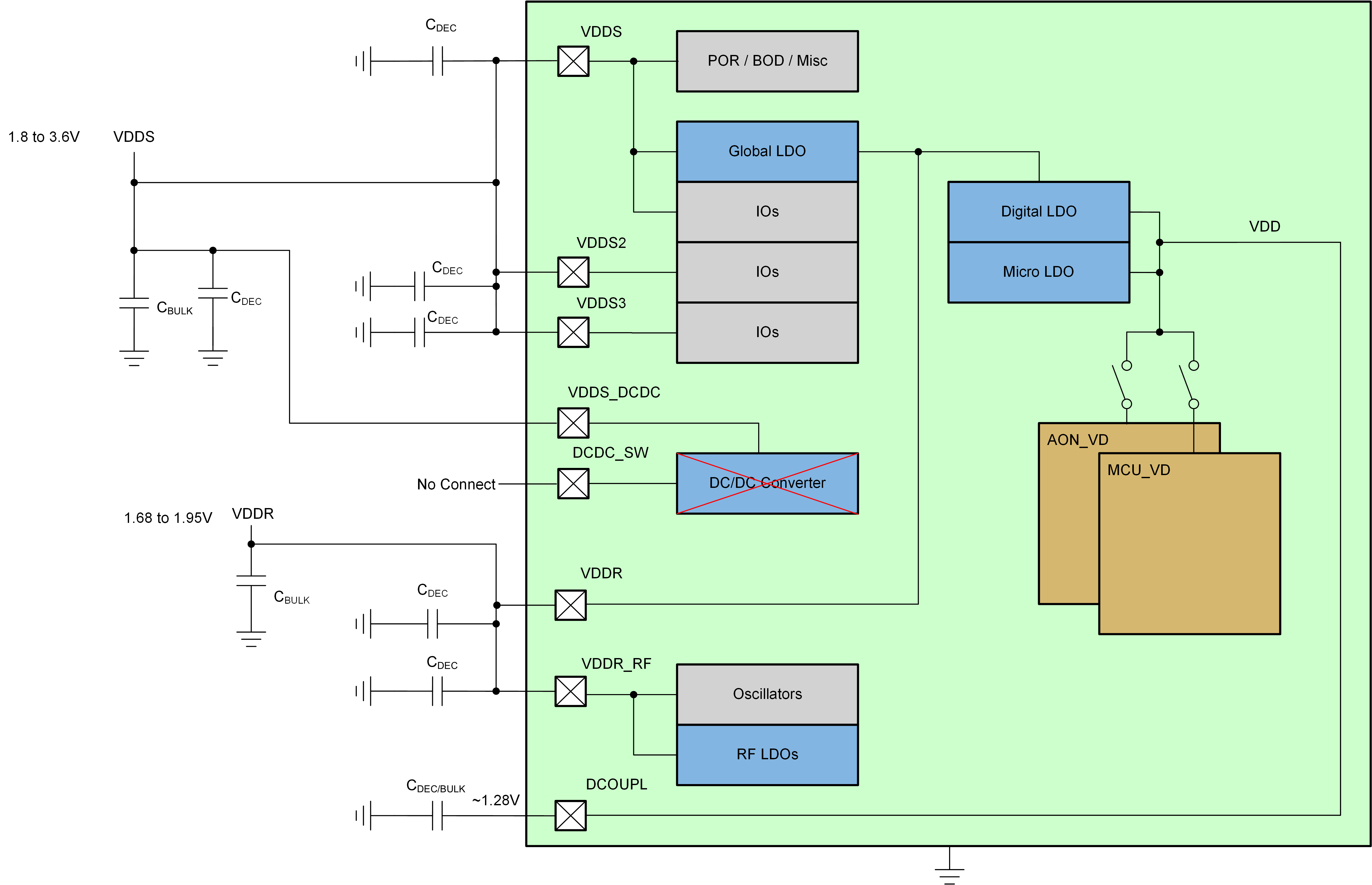
CC1354P10-6 Global LDO ModeFigure 11-2 Global LDO Mode
Note: The VDDS_DCDC pin is not present on all devices.

To save cost and PCB area the DC/DC inductor can be removed and VDDR can be supplied from the Global LDO at the cost of higher power consumption. In this mode a bulk capacitor on VDDR is still required and should be placed close to the VDDR pin. The VDDS_DCDC-pin must be connected to VDDS and the DCDC_SW should be left floating to avoid short circuiting VDDS if the DC/DC converter is mistakenly enabled from software. The VDDS bulk capacitor does not need to be close to the VDDS_DCDC pin and should rather be placed close to the VDDS pin.

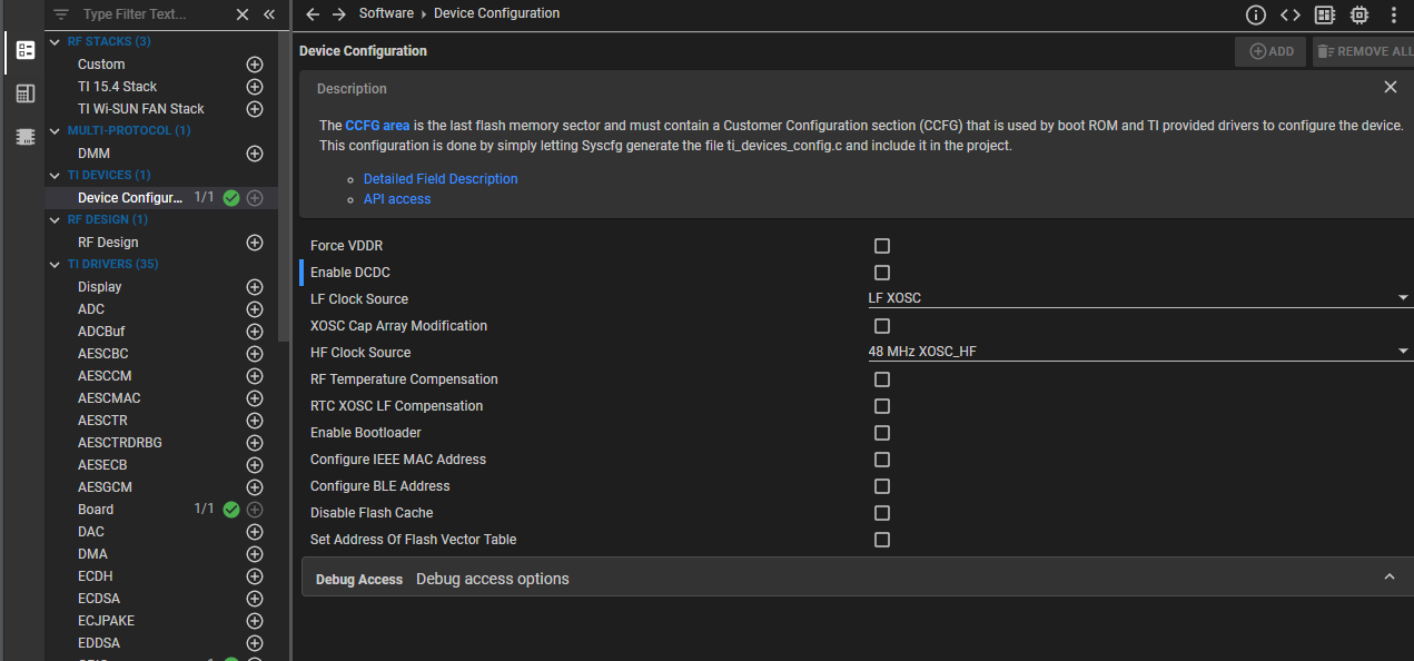
The software setup required to use the DCDC converter or the GLDO operation is done in the Customer Configuration (CCFG) register bank.

For devices that use SDK up to version 5.x (CC2640R2), the settings below must be made to the file ccfg.c.

#ifndef SET_CCFG_MODE_CONF_DCDC_RECHARGE       
// #define SET_CCFG_MODE_CONF_DCDC_RECHARGE    0x0   // Use the DC/DC during recharge in powerdown 
#define SET_CCFG_MODE_CONF_DCDC_RECHARGE       0x1   // Do not use the DC/DC during recharge in powerdown
#endif
#ifndef SET_CCFG_MODE_CONF_DCDC_ACTIVE
// #define SET_CCFG_MODE_CONF_DCDC_ACTIVE      0x0   // Use the DC/DC during active mode
#define SET_CCFG_MODE_CONF_DCDC_ACTIVE         0x1   // Do not use the DC/DC during active mode 
#endif

For devices that use SDK version 6.x and above, this is set up in the section TI DEVICES followed by Device Configuration of the Sysconfig file as indicated in the following image.
CC1354P10-6