SWRS205F March 2017 – December 2024 CC3120MOD
PRODUCTION DATA
- 1
- 1 Features
- 2 Applications
- 3 Description
- 4 Functional Block Diagrams
- 5 Device Comparison
- 6 Terminal Configuration and Functions
-
7 Specifications
- 7.1 Absolute Maximum Ratings
- 7.2 ESD Ratings
- 7.3 Recommended Operating Conditions
- 7.4 Current Consumption Summary
- 7.5 TX Power and IBAT versus TX Power Level Settings
- 7.6 Brownout and Blackout Conditions
- 7.7 Electrical Characteristics
- 7.8 WLAN Receiver Characteristics
- 7.9 WLAN Transmitter Characteristics
- 7.10 Reset Requirement
- 7.11 Thermal Resistance Characteristics for MOB Package
- 7.12 Timing and Switching Characteristics
- 7.13 External Interfaces
- 8 Detailed Description
- 9 Applications, Implementation, and Layout
- 10Environmental Requirements and Specifications
- 11Device and Documentation Support
- 12Revision History
- 13Mechanical, Packaging, and Orderable Information
7.13.1 SPI Host Interface
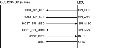
The device interfaces to an external host using the SPI. The CC3120MOD module can interrupt the host using the HOST_INTR line to initiate the data transfer over the interface. The SPI host interface can work up to a speed of 20 MHz.
Figure 7-8 shows the SPI host interface.
 Figure 7-8 SPI Host Interface
Table 7-4 lists the SPI host interface pins.
Table 7-4 SPI Host Interface
| PIN NAME | DESCRIPTION |
|---|---|
| HOST_SPI_CLK | Clock (up to 20 MHz) from MCU host to CC3120MOD module |
| HOST_SPI_nCS | CS (active low) signal from MCU host to CC3120MOD module |
| HOST_SPI_MOSI | Data from MCU host to CC3120MOD module |
| HOST_INTR | Interrupt from CC3120MOD module to MCU host |
| HOST_SPI_MISO | Data from CC3120MOD module to MCU host |
| nHIB | Active-low signal that commands the CC3120MOD module to enter hibernate mode (lowest power state) |
Figure 7-9 shows the host SPI timing diagram.
 Figure 7-9 Host SPI Timing
Table 7-5 lists the host SPI timing parameters.
Table 7-5 Host SPI Timing Parameters
| PARAMETER NUMBER | DESCRIPTION | MIN | MAX | UNIT | |
|---|---|---|---|---|---|
| T1 | F(1) | Clock frequency at VBAT = 3.3 V | 20 | MHz | |
| Clock frequency at VBAT = 2.3 V | 12 | ||||
| T2 | tclk(1)(2) | Clock period | 50 | ns | |
| T3 | tLP(1) | Clock low period | 25 | ns | |
| T4 | tHT(1) | Clock high period | 25 | ns | |
| T5 | D(1) | Duty cycle | 45% | 55% | |
| T6 | tIS(1) | RX data setup time | 4 | ns | |
| T7 | tIH(1) | RX data hold time | 4 | ns | |
| T8 | tOD(1) | TX data output delay | 20 | ns | |
| T9 | tOH(1) | TX data hold time | 24 | ns | |
(1) The timing parameter has a maximum load of 20 pf at 3.3 V.
(2) Ensure that nCS (active-low signal) is asserted 10 ns before the clock is toggled. The nCS signal can be deasserted 10 ns after the clock edge.