SWRS205F March   2017  – December 2024 CC3120MOD

PRODUCTION DATA  

  1.   1
  2. Features
  3. Applications
  4. Description
  5. Functional Block Diagrams
  6. Device Comparison
    1. 5.1 Related Products
  7. Terminal Configuration and Functions
    1. 6.1 CC3120MOD Pin Diagram
    2. 6.2 Pin Attributes
      1.      11
    3. 6.3 Connections for Unused Pins
  8. Specifications
    1. 7.1  Absolute Maximum Ratings
    2. 7.2  ESD Ratings
    3. 7.3  Recommended Operating Conditions
    4. 7.4  Current Consumption Summary
    5. 7.5  TX Power and IBAT versus TX Power Level Settings
    6. 7.6  Brownout and Blackout Conditions
    7. 7.7  Electrical Characteristics
    8. 7.8  WLAN Receiver Characteristics
    9. 7.9  WLAN Transmitter Characteristics
    10. 7.10 Reset Requirement
    11. 7.11 Thermal Resistance Characteristics for MOB Package
    12. 7.12 Timing and Switching Characteristics
      1. 7.12.1 Power-Up Sequencing
      2. 7.12.2 Power-Down Sequencing
      3. 7.12.3 Device Reset
      4. 7.12.4 Wakeup From HIBERNATE Mode Timing
    13. 7.13 External Interfaces
      1. 7.13.1 SPI Host Interface
      2. 7.13.2 Host UART Interface
        1. 7.13.2.1 5-Wire UART Topology
        2. 7.13.2.2 4-Wire UART Topology
        3. 7.13.2.3 3-Wire UART Topology
      3. 7.13.3 External Flash Interface
  9. Detailed Description
    1. 8.1 Overview
    2. 8.2 Module Features
      1. 8.2.1 WLAN
      2. 8.2.2 Network Stack
        1. 8.2.2.1 Security
      3. 8.2.3 Host Interface and Driver
      4. 8.2.4 System
    3. 8.3 Power-Management Subsystem
      1. 8.3.1 VBAT Wide-Voltage Connection
    4. 8.4 Low-Power Operating Modes
      1. 8.4.1 Low-Power Deep Sleep
      2. 8.4.2 Hibernate
      3. 8.4.3 Shutdown
    5. 8.5 Restoring Factory Default Configuration
    6. 8.6 Device Certification and Qualification
      1. 8.6.1 FCC Certification and Statement
      2. 8.6.2 Industry Canada (IC) Certification and Statement
      3. 8.6.3 ETSI/CE Certification
      4. 8.6.4 Japan MIC Certification
      5. 8.6.5 SRRC Certification and Statement
    7. 8.7 Module Markings
    8. 8.8 End Product Labeling
    9. 8.9 Manual Information to the End User
  10. Applications, Implementation, and Layout
    1. 9.1 Application Information
      1. 9.1.1 Typical Application
      2. 9.1.2 Power Supply Decoupling and Bulk Capacitors
      3. 9.1.3 Reset
      4. 9.1.4 Unused Pins
    2. 9.2 PCB Layout Guidelines
      1. 9.2.1 General Layout Recommendations
      2. 9.2.2 RF Layout Recommendations
      3. 9.2.3 Antenna Placement and Routing
      4. 9.2.4 Transmission Line Considerations
  11. 10Environmental Requirements and Specifications
    1. 10.1 Temperature
      1. 10.1.1 PCB Bending
    2. 10.2 Handling Environment
      1. 10.2.1 Terminals
      2. 10.2.2 Falling
    3. 10.3 Storage Condition
      1. 10.3.1 Moisture Barrier Bag Before Opened
      2. 10.3.2 Moisture Barrier Bag Open
    4. 10.4 Baking Conditions
    5. 10.5 Soldering and Reflow Condition
  12. 11Device and Documentation Support
    1. 11.1 Device Nomenclature
    2. 11.2 Development Tools and Software
    3. 11.3 Firmware Updates
    4. 11.4 Documentation Support
    5. 11.5 Trademarks
    6. 11.6 Electrostatic Discharge Caution
    7. 11.7 Glossary
  13. 12Revision History
  14. 13Mechanical, Packaging, and Orderable Information
    1. 13.1 Mechanical, Land, and Solder Paste Drawings
    2. 13.2 Package Option Addendum
      1. 13.2.1 Packaging Information
    3. 13.3 Tape and Reel Information
      1. 13.3.1 Tape and Reel Specification

Power-Up Sequencing

For proper start-up of the CC3120MOD module, perform the recommended power-up sequencing as follows:

  1. Tie VBAT1 (pin 37) and VBAT2 (pin 40) together on the board.
  2. Hold the nRESET pin low while the supplies are ramping up.

Figure 7-6 shows the reset timing diagram for the first-time power-up and reset removal.
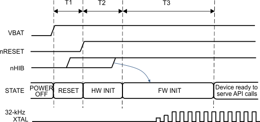
CC3120MOD First-Time Power-Up and Reset Removal Timing DiagramFigure 7-6 First-Time Power-Up and Reset Removal Timing Diagram


Table 7-2 describes the timing requirements for the first-time power-up and reset removal.

Table 7-2 First-Time Power-Up and Reset Removal Timing Requirements
ITEMNAMEDESCRIPTIONMINTYPMAXUNIT
T1Supply settling timeDepends on application board power supply, decoupling capacitor, and so on3ms
T2Hardware wake-up time25ms
T3Initialization timeInternal 32-kHz XTAL settling plus firmware initialization time plus radio calibration1.35s