TIDT236 March 2022 TPS7H1101A-SP
3.2 Output Voltage Ripple
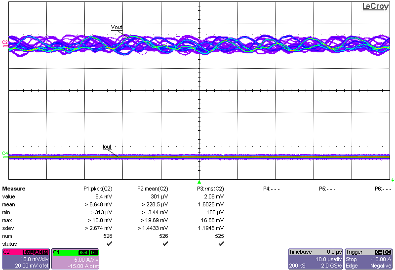
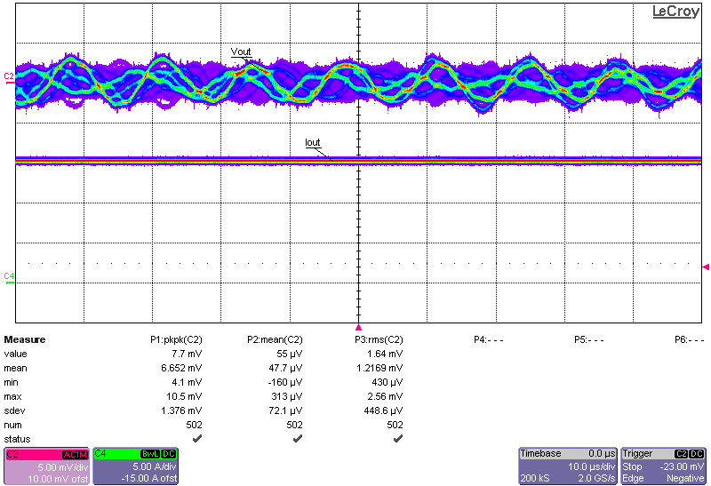
Figure 3-5 to Figure 3-8 show the output voltage ripple. The images are taken at 12-V input, –0.2-V and –0.6-V outputs both at no load and 15-A load conditions. The waveforms were captured with infinite persistence being enabled and measurements were made for the peak-to-peak, mean, and RMS values of the output voltage ripple.
 Figure 3-5 Output Voltage Ripple, 12-V Input, –0.2-V
Output, No Load
 Figure 3-6 Output Voltage Ripple, 12-V Input, –0.2-V
Output, 15-A Load
 Figure 3-7 Output Voltage Ripple, 12-V Input, –0.6-V
Output, No Load
 Figure 3-8 Output Voltage Ripple, 12-V Input, –0.6-V
Output, 15-A Load