TIDUE53I march   2018  – july 2023 TMS320F28P550SJ , TMS320F28P559SJ-Q1


  1.   1
  2.   Description
  3.   Resources
  4.   Features
  5.   Applications
  6.   6
  7. 1System Description
    1. 1.1 Key System Specifications
  8. 2System Overview
    1. 2.1 Block Diagram
    2. 2.2 Highlighted Products
      1. 2.2.1  UCC21710
      2. 2.2.2  UCC5320
      3. 2.2.3  TMS320F28379D
      4. 2.2.4  AMC1305M05
      5. 2.2.5  OPA4340
      6. 2.2.6  LM76003
      7. 2.2.7  PTH08080W
      8. 2.2.8  TLV1117
      9. 2.2.9  OPA350
      10. 2.2.10 UCC14240
    3. 2.3 System Design Theory
      1. 2.3.1 Three-Phase T-Type Inverter
        1. 2.3.1.1 Architecture Overview
        2. 2.3.1.2 LCL Filter Design
        3. 2.3.1.3 Inductor Design
        4. 2.3.1.4 SiC MOSFETs Selection
        5. 2.3.1.5 Loss Estimations
        6. 2.3.1.6 Thermal Considerations
      2. 2.3.2 Voltage Sensing
      3. 2.3.3 Current Sensing
      4. 2.3.4 System Power Supplies
        1. 2.3.4.1 Main Input Power Conditioning
        2. 2.3.4.2 Isolated Bias Supplies
      5. 2.3.5 Gate Drivers
        1. 2.3.5.1 1200-V SiC MOSFETs
        2. 2.3.5.2 650-V SiC MOSFETs
        3. 2.3.5.3 Gate Driver Bias Supply
      6. 2.3.6 Control Design
        1. 2.3.6.1 Current Loop Design
        2. 2.3.6.2 PFC DC Bus Voltage Regulation Loop Design
  9. 3Hardware, Software, Testing Requirements, and Test Results
    1. 3.1 Required Hardware and Software
      1. 3.1.1 Hardware
        1. 3.1.1.1 Test Hardware Required
        2. 3.1.1.2 Microcontroller Resources Used on the Design (TMS320F28379D)
        3. 3.1.1.3 F28377D, F28379D Control-Card Settings
        4. 3.1.1.4 Microcontroller Resources Used on the Design (TMS320F280039C)
      2. 3.1.2 Software
        1. 3.1.2.1 Getting Started With Firmware
          1. 3.1.2.1.1 Opening the CCS project
          2. 3.1.2.1.2 Digital Power SDK Software Architecture
          3. 3.1.2.1.3 Interrupts and Lab Structure
          4. 3.1.2.1.4 Building, Loading and Debugging the Firmware
        2. 3.1.2.2 Protection Scheme
        3. 3.1.2.3 PWM Switching Scheme
        4. 3.1.2.4 ADC Loading
    2. 3.2 Testing and Results
      1. 3.2.1 Lab 1
      2. 3.2.2 Testing Inverter Operation
        1. 3.2.2.1 Lab 2
        2. 3.2.2.2 Lab 3
        3. 3.2.2.3 Lab 4
      3. 3.2.3 Testing PFC Operation
        1. 3.2.3.1 Lab 5
        2. 3.2.3.2 Lab 6
        3. 3.2.3.3 Lab 7
      4. 3.2.4 Test Setup for Efficiency
      5. 3.2.5 Test Results
        1. 3.2.5.1 PFC Mode - 230 VRMS, 400 V L-L
          1. 3.2.5.1.1 PFC Start-up – 230 VRMS, 400 L-L AC Voltage
          2. 3.2.5.1.2 Steady State Results at 230 VRMS, 400 V L-L - PFC Mode
          3. 3.2.5.1.3 Efficiency and THD Results at 220 VRMS, 50 Hz – PFC Mode
          4. 3.2.5.1.4 Transient Test With Step Load Change
        2. 3.2.5.2 PFC Mode - 120 VRMS, 208 V L-L
          1. 3.2.5.2.1 Steady State Results at 120 VRMS, 208 V-L-L - PFC Mode
          2. 3.2.5.2.2 Efficiency and THD Results at 120 VRMS - PFC Mode
        3. 3.2.5.3 Inverter Mode
          1. 3.2.5.3.1 Inverter Closed Loop Results
          2. 3.2.5.3.2 Efficiency and THD Results - Inverter Mode
          3. 3.2.5.3.3 Inverter - Transient Test
      6. 3.2.6 Open Loop Inverter Test Results
  10. 4Design Files
    1. 4.1 Schematics
    2. 4.2 Bill of Materials
    3. 4.3 PCB Layout Recommendations
      1. 4.3.1 Layout Prints
    4. 4.4 Altium Project
    5. 4.5 Gerber Files
    6. 4.6 Assembly Drawings
  11. 5Trademarks
  12. 6About the Authors
  13. 7Revision History

Thermal Considerations

The loss estimations can also allow the heat output of the design to be characterized. Any electrical loss in the system is converted to waste heat.

Thermal simulations where performed using the physical layout of the design, as well as the expected energy losses. An off the shelf heat sink from Wakefield-Vette (OMNI-UNI-18-50) was selected to simplify the design process and provide a starting reference point for understanding the thermal performance. Use this data as a starting point for a thermal design, and not a fully-validated design.

The system was simulated using a worse-than-calculated thermal output of 10 W per switching device. This meant 120 W of total power dissipation across all three phases. Figure 2-33 and Figure 2-34 show the thermal simulation results with no fans.
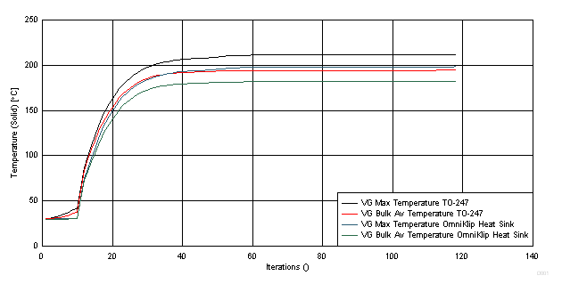
GUID-2DB8DD89-7216-4DD8-B866-12E7E2E5D64D-low.gifFigure 2-33 Simulated Temperature vs Time
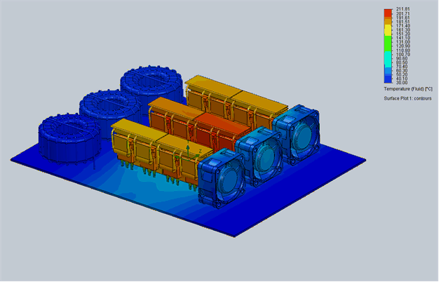
GUID-7A3DDEB3-A8C3-4CD8-A9DE-1BDAE55C8806-low.gifFigure 2-34 Passive Thermal Simulation Result

In this simulation, with only natural convection and small off the shelf heat sinks, the TO-247 package of the MOSFETs reaches a maximum temperature of 215°C, and the SiC MOSFET reaches 197°C. These temperatures are both outside the maximum allowed temperature range of the devices.

Figure 2-35 shows the next simulation, which includes active airflow and full ducting of the heat generating devices. This airflow reduces the maximum temperature of the MOSFET under a 130% load to be 130°C. This temperature is within the design constraint of the 175°C junction temperature of the C3M0060065D, which is the major heat generator. Please contact wakefield-Vette for details on the thermal simulation.
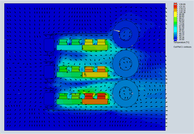
GUID-95D90092-93CB-4AE3-8088-84A3851DC9A0-low.gifFigure 2-35 Active Ducted Thermal Simulation