TIDUES0E June 2019 – April 2024 TMS320F28P550SG , TMS320F28P550SJ , TMS320F28P559SJ-Q1
- 1
- Description
- Resources
- Features
- Applications
- 6
- 1System Description
- 2System Overview
- 3Circuit Description
- 4Hardware, Software, Testing Requirements, and Test Results
- 5Design Files
- 6Related Documentation
- 7Terminology
- 8About the Author
- 9Revision History
4.4.5 Lab 5
Figure 4-40 shows test setup for lab 5 (Open Loop voltage - Reverse power flow).

Figure 4-40 Lab 5 Test Setup
In this setup, the DC source is connected to the secondary side and the resistive load is connected to the primary side.

Figure 4-40 Lab 5 Test Setup
Compile the project by selecting Lab 5: Open Loop PWM, Sec to Prim Power Flow in the drop-down menu of Project Options from PowerSUITE GUI. Make sure current and voltage limits are set per operating conditions.
#if DAB_LAB == 5
#define DAB_CONTROL_RUNNING_ON C28X_CORE
#define DAB_POWER_FLOW DAB_POWER_FLOW_SEC_PRI
#define DAB_INCR_BUILD DAB_OPEN_LOOP_BUILD
#define DAB_CONTROL_MODE  DAB_VOLTAGE_MODE
#define DAB_TEST_SETUP DAB_TEST_SETUP_RES_LOAD
#define DAB_PROTECTION DAB_PROTECTION_ENABLED
#define DAB_SFRA_TYPE  2
#define DAB_SFRA_AMPLITUDE (float32_t)DAB_SFRA_INJECTION_AMPLITUDE_LEVEL2
#endif- Run the project by clicking the green run button in CCS.
- Populate the required variables
in the watch window by loading JavaScript
setupdebugenv_lab5.jsin the scripting console.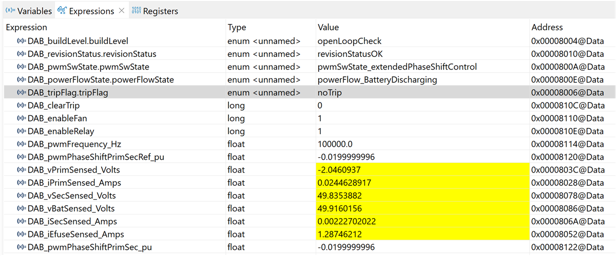 Figure 4-41 Lab 5 - Watch
View
 - Enable fans and relays by writing
"1" into
DAB_enableFanandDAB_enableRelay. - Enable PWM by writing “1” to the
DAB_clearTripvariable. - Vary phase shift slowly in steps
of 0.002 pu by writing to
DAB_pwmPhaseShiftPrimSec_puand observe the change in voltage at the output of converter.Note: The negative sign in the phase shift value is required for the reverse power flow. - Before increasing voltages validate primary side overvoltage protection.
- Set VPRIM_TRIP to 50 V.
- Slowly increase (negative) phase
shift and observe trip when voltage hits 50 V.
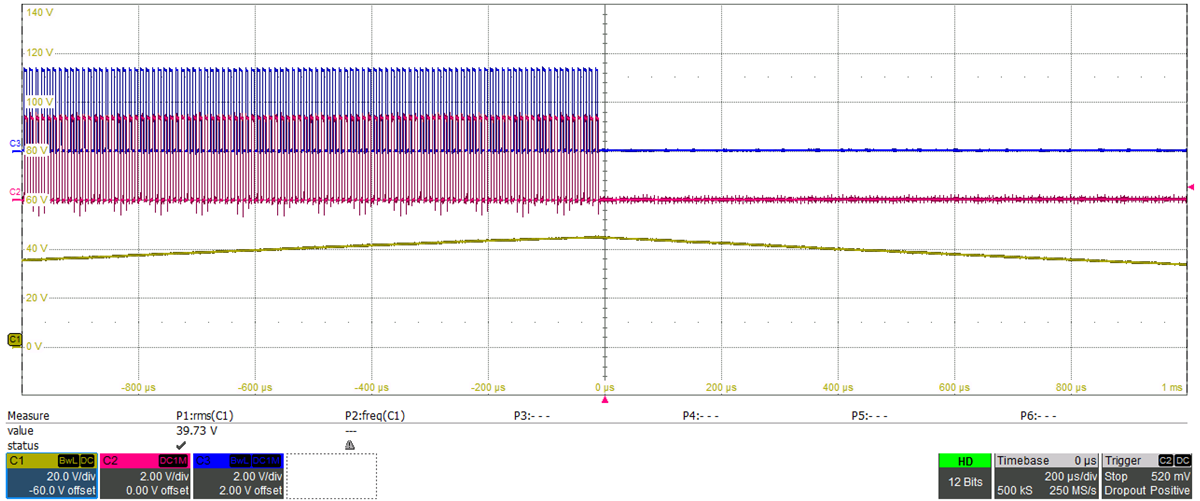 Figure 4-42 Lab 5 - Primary Side
Overvoltage Protection
 - After verifying that overvoltage protection is working, set VPRIM_TRIP back to 1000 V.
- Now voltage on the secondary
side can be slowly increased and phase shift can be modified to observe the
primary side voltage and current.
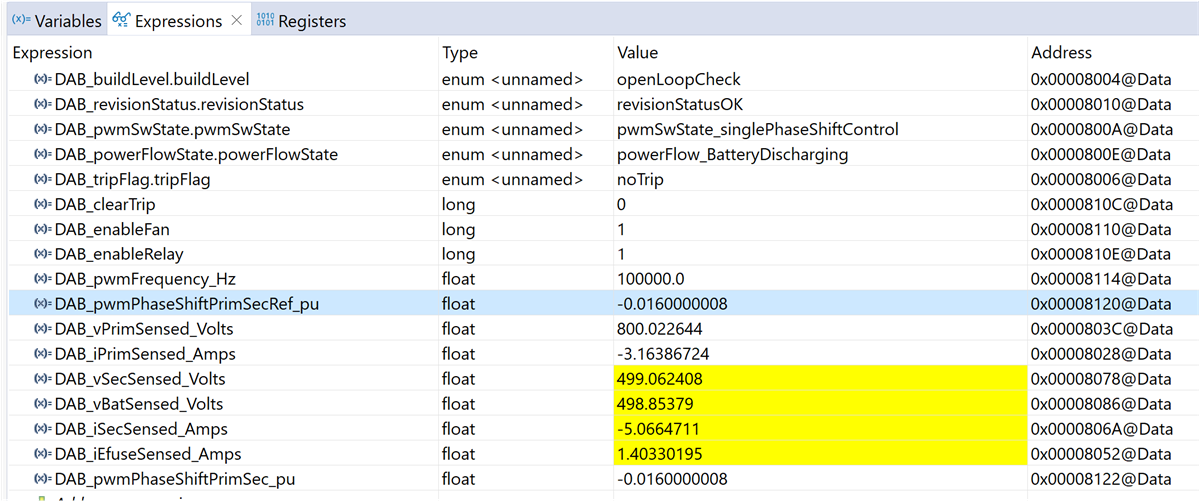 Figure 4-43 Lab 5 Expression
Window High Voltage
- Measure SFRA Plant for Voltage
Loop
- Follow the same
instructions as in Lab 2.
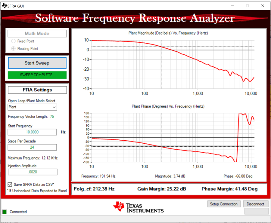 Test Condition: VIN = 350 V, VOUT = 550 V, IOUT = 9 A.Figure 4-44 Lab 5 - SFRA Plant Plot for the Open Voltage Loop Test
VIN refers to secondary side voltage, VOUT and IOUT refer to primary side voltage and current in reverse direction (DAB_IprimSensed_Amps = –9 A ).
- Follow the same
instructions as in Lab 2.
- Measure SFRA Plant for Current Loop
- Follow the same steps as
in Lab 2.
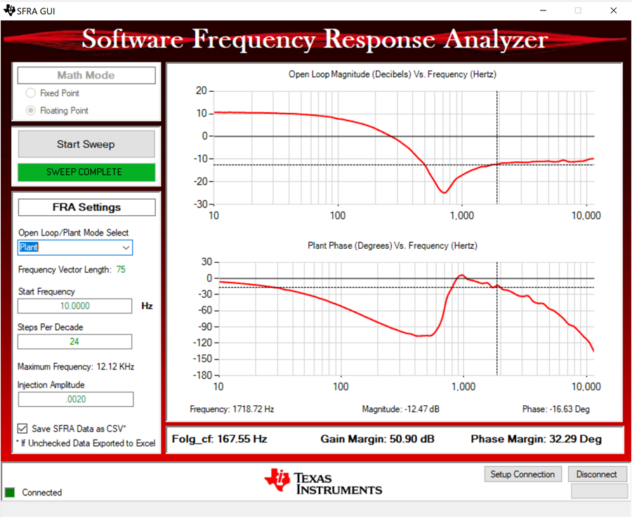 Test Condition: VIN = 350 V, VOUT = 550 V, IOUT = 9 A.Figure 4-45 Lab 5 - SFRA Plant Plot for the Open Current Loop Test
VIN refers to secondary side voltage, VOUT and IOUT refer to primary side voltage and current in reverse direction (DAB_IprimSensed_Amps = –9 A).
- Follow the same steps as
in Lab 2.