TIDUES0E June 2019 – April 2024 TMS320F28P550SG , TMS320F28P550SJ , TMS320F28P559SJ-Q1
- 1
- Description
- Resources
- Features
- Applications
- 6
- 1System Description
- 2System Overview
- 3Circuit Description
- 4Hardware, Software, Testing Requirements, and Test Results
- 5Design Files
- 6Related Documentation
- 7Terminology
- 8About the Author
- 9Revision History
3.7.2 Running Simulations
This section contains instructions for PLECS using the Blockset and standalone setup.
Instructions PLECS Blockset:
- Open both TIDA_010054_DAB_Converter_Parameters.m and TIDA_010054_DAB_Converter_Simulation.slx files in MATLAB
- Open the PLECS circuit in TIDA_010054_DAB_Converter_Simulation.slx
- Add the TIDA_010054_DAB_Converter_Models folder to the thermal library (File → PLECS Preferences → Thermal → (Press the plus sign))
- Run TIDA_010054_DAB_Converter_Parameters.m to populate parameters in the MATLAB workspace. These can be modified to simulate different operation points or to enable and disable extended-phase-shift control (EPS_EN = 1 or EPS_EN = 0)
- Run simulation either by pressing Run in TIDA_010054_DAB_Converter_Simulation.slx or by pressing Simulation → Run in the PLECS Simulation Deck
- Simulation can be observed in scopes and displays within the PLECS circuit
Instructions PLECS Standalone:
- Open the TIDA_010054_DAB_standalone.plecs file in PLECS
- Add the TIDA_010054_DAB_Converter_Models folder to the thermal library (File → PLECS Preferences → Thermal → (Press the plus sign))
- Initialization is found under Simulation → Simulation parameters → Initialization. These can be modified to simulate different operation points or to enable and disable extended-phase-shift control (EPS_EN = 1 or EPS_EN = 0)
- Run the simulation by pressing Simulation → Run in the PLECS Simulation Deck
- Simulation can be observed in scopes and displays within the PLECS circuit
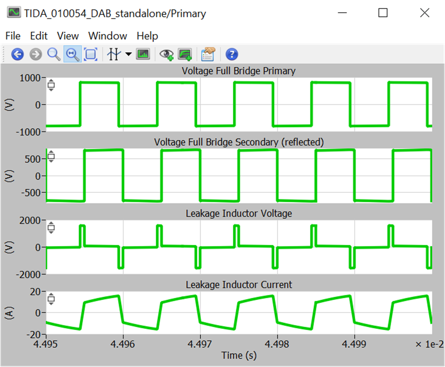
Figure 3-16 shows the primary scope. Use this scope to evaluate the switching waveforms.
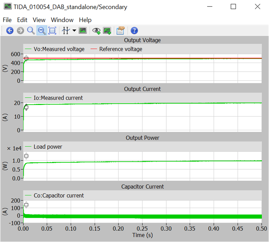
Figure 3-17 shows the secondary scope. Use this window to observe output voltage, current, and power, as well as the output voltage ripple and capacitor current.
 Figure 3-16 PLECS - Primary Scope
 Figure 3-17 PLECS - Secondary
Scope
Figure 3-17 PLECS - Secondary
ScopeNote: This simulation deck is for system
level evaluation. Not all parasitic effects can be simulated accurately. Simulation
results can vary from measurement results.
For example, SiC-FET manufacturer models do not include output capacitances. Therefore, soft-switching is achieved down to very light loads in simulation. Efficiencies under light load vary from actual measurements.
For example, SiC-FET manufacturer models do not include output capacitances. Therefore, soft-switching is achieved down to very light loads in simulation. Efficiencies under light load vary from actual measurements.