TIDUF52 December 2023 MSPM0L1303 , MSPM0L1304 , MSPM0L1305 , MSPM0L1306 , MSPM0L1343 , MSPM0L1344 , MSPM0L1345 , MSPM0L1346
- 1
- Description
- Resources
- Features
- Applications
- 6
- 1System Description
- 2System Overview
- 3Hardware, Software, Testing Requirements, and Test Results
- 4Design and Documentation Support
- 5About the Author
2.2.3.2 BPF
Figure 2-9 shows the schematic of the second stage of the AFE. The bandpass filter stage consists of an active high-pass filter utilizing the internal op amp (OPA1) in the M0L1306 with 6-MHz gain-bandwidth and an R-C low-pass filter. The high-pass stage makes sure any DC (low frequency) interference is removed (attenuated) without disturbing the modulated signal. The low-pass stage provides filtering to any high-frequency noise presented in the previous signal chain before demodulation. The high-pass filter gain and 3-dB high-pass pole frequency are given as:
The 3-dB low-pass frequency is given as:
The bias voltage of the BPF is selected as 1.65 V (VDD/2) generated by two 10-MΩ series resistors as shown in Figure 2-1 and also Figure 2-9.
 Figure 2-7 BPF Schematic
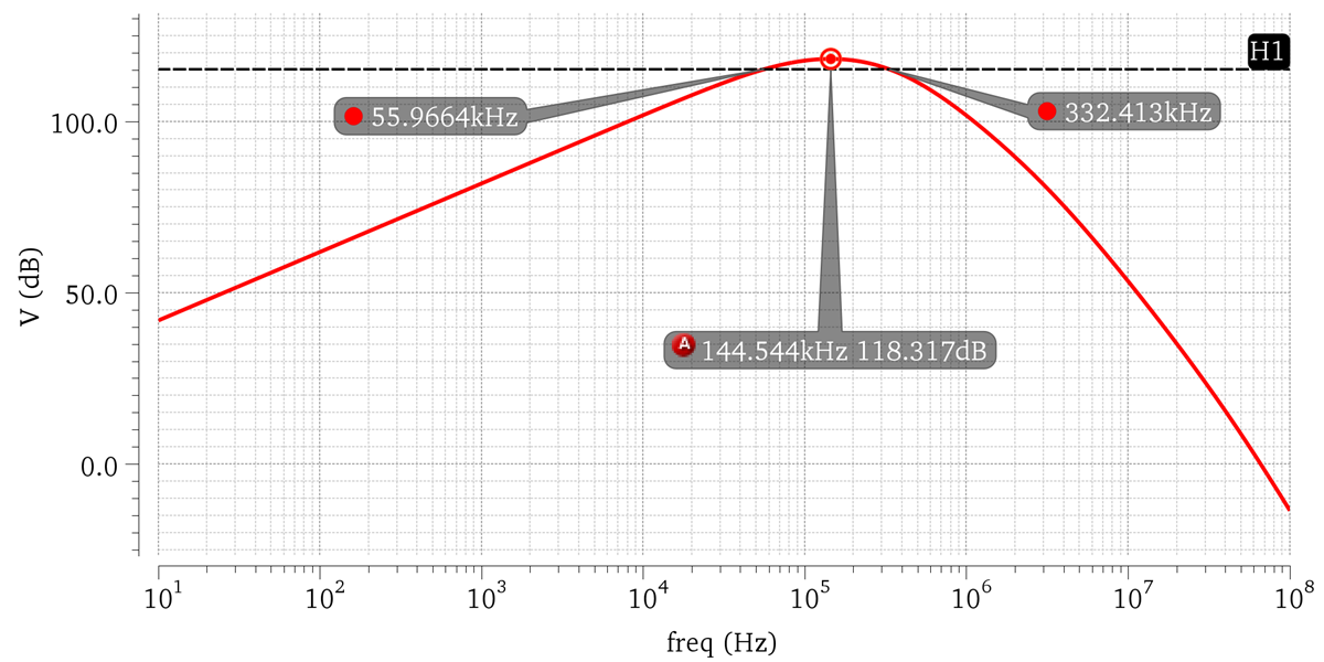
Figure 2-8 shows the simulated frequency response from input current to BPF output voltage of the combined TIA and BPF stages with the aforementioned design parameters. The peak gain is 118.3 dB (0.82 MΩ) at 144.5 kHz which is lower than the calculated gain of 4.5 × 249 kΩ = 1.12 MΩ due to the low damping factor of the simple poles and the spacing of the cutoff frequencies being less than one decade or more apart. The 3-dB bandpass cutoff frequency is at 56 kHz at the low side and 332 kHz at the high side. The frequency response shape can be simply modified by adjusting corresponding R, C values to satisfy specific design requirements on different modulation frequency selections.
 Figure 2-8 Frequency Magnitude Response of Combined TIA and BPF