TIDUF65 March 2024
- 1
- Description
- Resources
- Features
- Applications
- 6
- 1System Description
- 2System Overview
- 3System Design Theory
- 4Hardware, Software, Testing Requirements, and Test Results
- 5Performance Comparison with Competitor’s Device
- 6Design and Documentation Support
- 7About the Author
4.4.6 Power Supply Rejection Ratio
Power supply noise usually adds extra noise on the output voltage of the Hall sensor, which reduces the accuracy of the sensor. Power supply rejection ration (PSRR) is an important parameter for Hall sensors. In PSRR tests, a 300mV, 100kHz peak-to-peak ripple is injected to the TMCS1123 supply voltage. The output voltage ripple of the TMCS1123 shows the ability to reject the power supply ripple. In this test, a DC power supply and signal generator are used to generate this ripple. The block diagram is shown as Figure 4-24.
 Figure 4-24 PSRR Test Setup
In Figure 4-25, the purple curve is the injected voltage ripple with a 320mV peak-to-peak value and 100kHz frequency. The scope plot shows the both the reference voltage VREF and output voltage VOUT of TMCS1123 have the same frequency ripple. Record the VREF and VOUT in 100ms, measure the peak-to-peak value of the waveform in 100ms and compare the value with the results under no power-supply ripple.
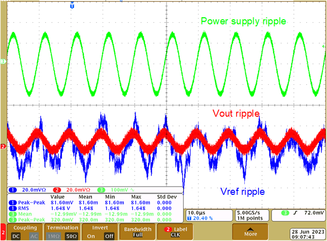 Figure 4-25 Power Supply Ripple, Reference
Voltage, Output Voltage Waveform
Figure 4-25 Power Supply Ripple, Reference
Voltage, Output Voltage WaveformThe results are shown in Figure 4-26 and Figure 4-27.
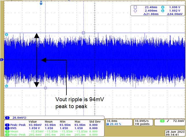 Figure 4-26 TMCS1123 Output Voltage vs
GND at High Supply Voltage Ripple
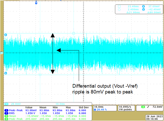 Figure 4-27 TMCS1123 Output Voltage vs
VREF High-Supply Voltage Ripple
Figure 4-27 TMCS1123 Output Voltage vs
VREF High-Supply Voltage RippleWhen the power supply ripple is added, the ripple of VOUT is 94mVPP and differential output voltage ripple of VOUT – VREF is 80mV, the differential output helps TMCS1123 to reduce output noise brought by power supply ripple and improve the measurement accuracy.
Plot the sampling data of the ADS7043 and AMC1035, which is shown in Figure 4-28 to Figure 4-31.
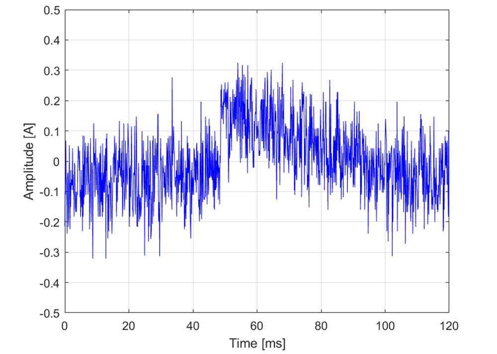 Figure 4-28 Output Noise With Supply
Voltage Ripple (Sampled With ADS7043 at 10kHz)
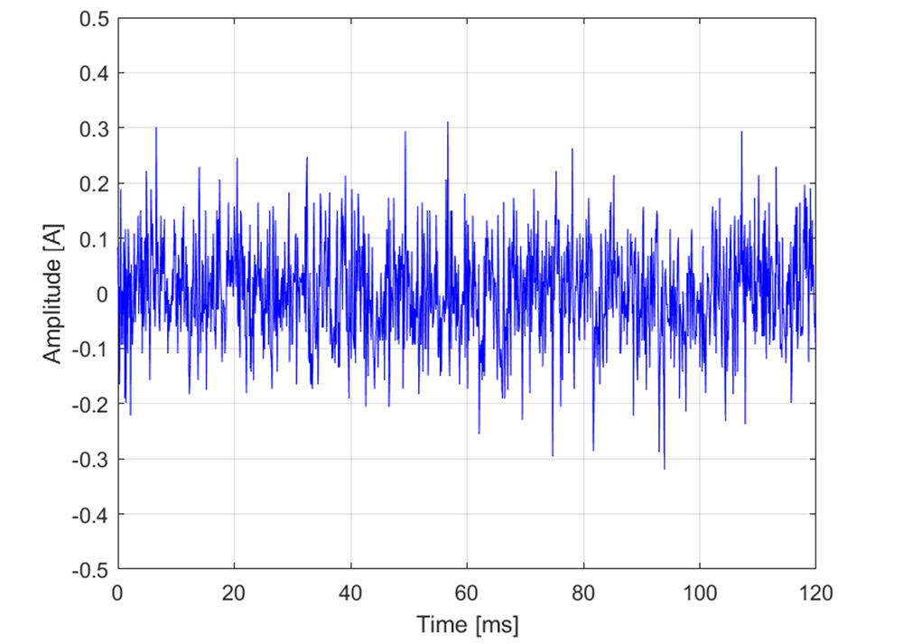 Figure 4-29 Output Noise no Supply
Voltage Ripple (Sampled With ADS7043 at 10kHz)
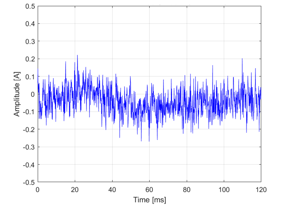 Figure 4-30 Output Noise With Supply
Voltage Ripple (Sampled With AMC1035 at 10kHz)
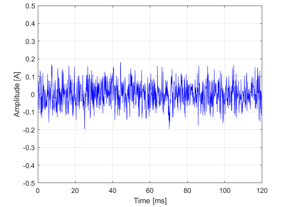 Figure 4-31 Output Noise With no
Supply Voltage Ripple (Sampled With AMC1035 at 10kHz)
Figure 4-31 Output Noise With no
Supply Voltage Ripple (Sampled With AMC1035 at 10kHz)For ADS7043, the peak-to-peak noise is around 600mA and for AMC1035, the value is around 450mA. These results are consistent with DC noise test results in Section 4.4.1.1. Using Delta-Sigma modulators can further reduce the influence from the power supply ripple.
The results show spectral aliasing due to higher signal frequency (100kHz) than sampling frequency (10kHz).