TIDUF82A August   2024  – November 2024 DRV8162 , INA241A , ISOM8710


  1.   1
  2.   Description
  3.   Resources
  4.   Features
  5.   Applications
  6.   6
  7. 1System Description
    1. 1.1 Reference Design Overview
    2. 1.2 Key System Specifications
  8. 2System Overview
    1. 2.1 Block Diagram
    2. 2.2 Design Considerations
      1. 2.2.1 Hardware Design
        1. 2.2.1.1 Power Stage Gate Driver
          1. 2.2.1.1.1 Gate Driver
          2. 2.2.1.1.2 Protection Features
          3. 2.2.1.1.3 VGVDD Definition
          4. 2.2.1.1.4 Strap Functions
        2. 2.2.1.2 Power Stage FETs
          1. 2.2.1.2.1 VGS versus RDS(ON)
        3. 2.2.1.3 Phase Current and Voltage Sensing
          1. 2.2.1.3.1 Phase Current
          2. 2.2.1.3.2 Phase Current – Bias Voltage Reference
          3. 2.2.1.3.3 Voltage
        4. 2.2.1.4 Host Processor Interface
        5. 2.2.1.5 Gate Drive Shutdown Path
        6. 2.2.1.6 System Diagnostic Measurements
          1. 2.2.1.6.1 Temperature Measurement
        7. 2.2.1.7 System Power Supply
          1. 2.2.1.7.1 12V Rail
          2. 2.2.1.7.2 3.3V Rail
      2. 2.2.2 Software Design
    3. 2.3 Highlighted Products
      1. 2.3.1 DRV8162L
      2. 2.3.2 INA241A
      3. 2.3.3 LMR38010
      4. 2.3.4 TMP6131
      5. 2.3.5 ISOM8710
  9. 3Hardware, Software Test Requirements and Test Results
    1. 3.1 Hardware Requirements
      1. 3.1.1 PCB Overview
      2. 3.1.2 Hardware Configuration
        1. 3.1.2.1 Prerequisites
        2. 3.1.2.2 Default Resistor and Jumper Configuration
        3. 3.1.2.3 Connector
          1. 3.1.2.3.1 Host Processor Interface
    2. 3.2 Test Setup
    3. 3.3 Test Results
      1. 3.3.1 Power Management
        1. 3.3.1.1 Power Up
        2. 3.3.1.2 Power Down
      2. 3.3.2 Gate Voltage and Phase Voltage
        1. 3.3.2.1 20 VDC
        2. 3.3.2.2 48 VDC
        3. 3.3.2.3 60 VDC
      3. 3.3.3 Digital PWM and Gate Voltage
      4. 3.3.4 Phase-Current Measurements
      5. 3.3.5 System Test Results
        1. 3.3.5.1 Thermal Analysis
  10. 4Design and Documentation Support
    1. 4.1 Design Files
      1. 4.1.1 Schematics
      2. 4.1.2 BOM
    2. 4.2 Tools and Software
    3. 4.3 Documentation Support
    4. 4.4 Support Resources
    5. 4.5 Trademarks
  11. 5About the Authors
  12. 6Revision History

Power Up

Figure 3-4 illustrates the TIDA-010956 power-up sequence.
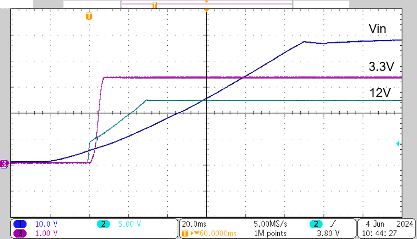
TIDA-010956 TIDA-010956 Power-Up
                    Sequence Figure 3-4 TIDA-010956 Power-Up Sequence

The power up sequence of the system is as follows: 48V VIN (CH1 in dark blue) goes above approximately 5V first, then LMR38010FDDAR starts providing the 12V rail (CH2 in light blue). When this 12V rail is approximately 5V, the 3.3V rail (CH3 in purple) is enabled.

The VIN has a slow ramp up while charging the VDC bus capacitors which are mainly of 330µF × 2 + 2.2µF × 20 and sum up to over 700µF. Another 180µF × 20 = 3.6mF needs to be added if a capacitor board is adopted.