TIDUF82A August   2024  – November 2024 DRV8162 , INA241A , ISOM8710


  1.   1
  2.   Description
  3.   Resources
  4.   Features
  5.   Applications
  6.   6
  7. 1System Description
    1. 1.1 Reference Design Overview
    2. 1.2 Key System Specifications
  8. 2System Overview
    1. 2.1 Block Diagram
    2. 2.2 Design Considerations
      1. 2.2.1 Hardware Design
        1. 2.2.1.1 Power Stage Gate Driver
          1. 2.2.1.1.1 Gate Driver
          2. 2.2.1.1.2 Protection Features
          3. 2.2.1.1.3 VGVDD Definition
          4. 2.2.1.1.4 Strap Functions
        2. 2.2.1.2 Power Stage FETs
          1. 2.2.1.2.1 VGS versus RDS(ON)
        3. 2.2.1.3 Phase Current and Voltage Sensing
          1. 2.2.1.3.1 Phase Current
          2. 2.2.1.3.2 Phase Current – Bias Voltage Reference
          3. 2.2.1.3.3 Voltage
        4. 2.2.1.4 Host Processor Interface
        5. 2.2.1.5 Gate Drive Shutdown Path
        6. 2.2.1.6 System Diagnostic Measurements
          1. 2.2.1.6.1 Temperature Measurement
        7. 2.2.1.7 System Power Supply
          1. 2.2.1.7.1 12V Rail
          2. 2.2.1.7.2 3.3V Rail
      2. 2.2.2 Software Design
    3. 2.3 Highlighted Products
      1. 2.3.1 DRV8162L
      2. 2.3.2 INA241A
      3. 2.3.3 LMR38010
      4. 2.3.4 TMP6131
      5. 2.3.5 ISOM8710
  9. 3Hardware, Software Test Requirements and Test Results
    1. 3.1 Hardware Requirements
      1. 3.1.1 PCB Overview
      2. 3.1.2 Hardware Configuration
        1. 3.1.2.1 Prerequisites
        2. 3.1.2.2 Default Resistor and Jumper Configuration
        3. 3.1.2.3 Connector
          1. 3.1.2.3.1 Host Processor Interface
    2. 3.2 Test Setup
    3. 3.3 Test Results
      1. 3.3.1 Power Management
        1. 3.3.1.1 Power Up
        2. 3.3.1.2 Power Down
      2. 3.3.2 Gate Voltage and Phase Voltage
        1. 3.3.2.1 20 VDC
        2. 3.3.2.2 48 VDC
        3. 3.3.2.3 60 VDC
      3. 3.3.3 Digital PWM and Gate Voltage
      4. 3.3.4 Phase-Current Measurements
      5. 3.3.5 System Test Results
        1. 3.3.5.1 Thermal Analysis
  10. 4Design and Documentation Support
    1. 4.1 Design Files
      1. 4.1.1 Schematics
      2. 4.1.2 BOM
    2. 4.2 Tools and Software
    3. 4.3 Documentation Support
    4. 4.4 Support Resources
    5. 4.5 Trademarks
  11. 5About the Authors
  12. 6Revision History

Power Down

During the power-down process, the VIN ramp down is also slow because the VIN has to discharge the > 700µF capacitance (see Figure 3-5).

As the VIN drops to approximately 7V, the 12V rail starts to power down. When this 12V rail gets to approximately 4V, the VIN shuts down the 3.3V rail. Then the remaining charge of the capacitors dissipates slowly.
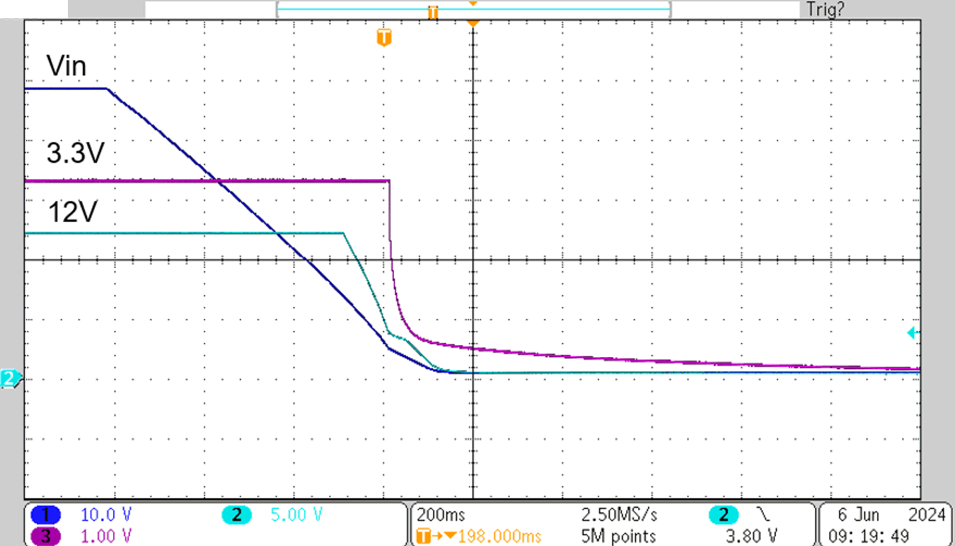
TIDA-010956 TIDA-010956 Power-Down
                    Sequence Figure 3-5 TIDA-010956 Power-Down Sequence

Table 3-7 shows the system status when the current is a 12V rail.

Table 3-7 12V Rail Current in Various System Status
MEASUREMENT SYSTEM STATUS 12V RAIL CURRENT
Current (mA) Idle (Gate driver disabled) 73.5
Current (mA) 16kHz PWM 125.4
Note: By default, in this design the C2000 LaunchPad is supposed to be powered up by the TIDA-010956 with the 3.3V supply through a 0Ω resistor (R29). Remove the JP1 (5V power supply from the PC USB) on the LAUNCHXL-F280039C before applying VIN.