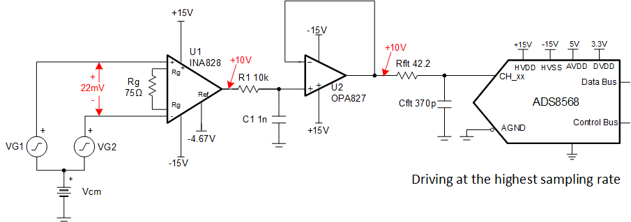
Circuit for driving an ADC with an instrumentation amplifier in high gain
| Input | ADC Input | Digital Output ADS8568 |
|---|---|---|
| VinDiffMin = –8mV | CH_x = –10V | 8000H |
| VinDiffMax = +22mV | CH_x = +10V | 7FFFH |
| AVDD | Vee | Vdd | |
|---|---|---|---|
| 5.0V | 3.3V | +15V | –15V |
Design Description
Instrumentation amplifiers are optimized for low noise, low offset, low drift, high CMRR and high accuracy but these instrument amplifiers are not able to drive a precision ADC to settle the signal properly during the acquisition time of ADC. This design shows an example of how to set the gain and offset shift to amplify a low level asymmetric input signal. Also, the high gain limits the INA828 instrumentation amplifier bandwidth, so an OPA827 op amp is used as a buffer so that the ADS8568 full sampling rate can be achieved. A related cookbook circuit shows a simplified approach that does not include the wide bandwidth buffer (Driving High Voltage SAR ADC with an Instrumentation Amplifier), this simplified approach has limited sampling rate as compared to the buffered design in this document. Also Driving High Voltage SAR ADC with a Buffered Instrumentation Amplifier, analyzes this design in unity gain. This circuit implementation is applicable to all Bridge Transducers in PLC’s and Analog Input Modules that require precision signal-processing and data-conversion.
| Specification | Goal | Calculated | Simulated |
|---|---|---|---|
| Transient Settling Error | >0.5 LSB (152µV) | NA | 0.36µV |
| Noise | 1.1mV | 1.14mV | |
| System Offset Error | 33.6mV | NA | |
| System Offset Drift | 334µV/°C | NA | |
| System Gain Error | 0.53% | NA | |
| System Gain Drift | 54.2ppm/°C | NA |
Design Notes
- The bandwidth of instrumentation amplifiers is typically not enough to drive SAR data converters at a higher data rate. This is especially true when the instrumentation amplifier is in high gain. so a wide bandwidth driver is needed because the SAR ADC with switched-capacitor input structure has an input capacitor that needs to be fully charged during each acquisition time. The OPA827 buffer is added to allow the ADC to run at full sampling rate (ADS8568 510kSPS for parallel interface).
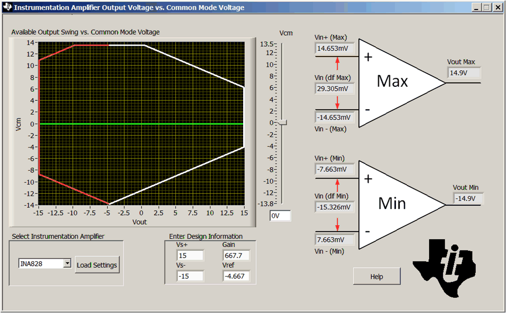
- Check the common-mode range of the amplifier using the Common-Mode Input Range Calculator for Instrumentation Amplifiers software tool.
- Select COG capacitors for C1 and Cfilt to minimize distortion.
- The gain set resistor, Rg, are 0.1% 20ppm/°C film resistors or better for low gain error and low gain drift.
- The TI Precision Labs video series covers the method for selecting the driver amplifier and the charge bucket circuit Rfilt and Cfilt. See Introduction of SAR ADC Front-End Component Selection for details.
- Set the cutoff of the filter between the op amp and instrumentation amplifier for anti aliasing and to minimize noise. See Aliasing and Anti-aliasing Filters for more details on aliasing and anti-aliasing filters.
- Because of the high instrumentation amplifier gain, the DC errors (offset, gain, and drift) are significant. Calibration is a good approach to minimizing these errors. See Understanding and Calibrating the Offset and Gain for ADC Systems for more details on calibration.
Component Selection
- Find the gain based on differential
input signal and the ADS8568
full-scale input range.
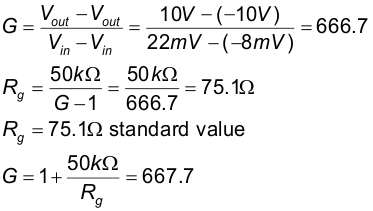
- The input signal in this design is
±10-V high voltage signal, so the gain of INA828 are
set to 1 and no gain resistor (Rg) is needed.
- Use the Common-Mode
Input Range Calculator for Instrumentation Amplifiers to
determine if the INA826 is violating the common-mode range. The common-mode
calculator in the following figure indicates that the output swing is ±14.9V for
a 0-V common-mode input.
- Find the value for Cfilt, and Rfilt using TINA-TI SPICE and the methods described in Introduction of SAR ADC Front-End Component Selection videos. The value of Rfilt and Cfilt shown in this document works for these circuits; however, when using different amplifiers new values are needed that are found using TINA-TI SPICE.
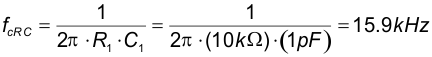
- Select the RC filter between the
INA828 and OPA827 based on your system requirements (fcRC = 15.9kHz
in this example).
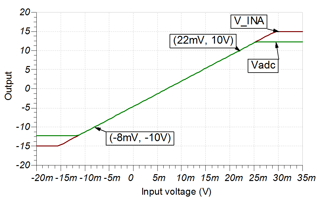
DC Transfer Characteristics
The following graph shows a linear output response for inputs from differential –10V to +10V. See Determining a SAR ADC’s Linear Range when using Instrumentation Amplifiers for detailed theory on this subject. The full-scale range (FSR) of the ADC falls within the linear range of the Instrumentation Amplifier.
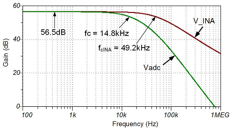
AC Transfer Characteristics
The bandwidth for this design is simulated to be 14.8kHz and the gain is 56.4dB (667.7V/V). The bandwidth limit is set by a combination RC filter (fcRC = 15.9kHz) and the instrumentation amplifier (fcINA=49.2kHz).
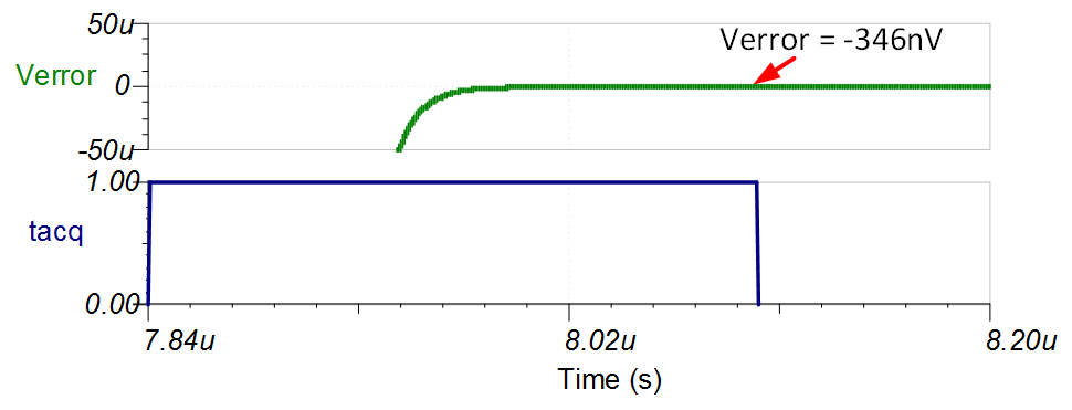
Transient ADC Input Settling Simulation (510kSPS)
The OPA827 buffer (22-MHz GBW) is used because it is capable of responding to the rapid transients from the charge kickback of the ADS8568. The op-amp buffer allows the system to achieve the ADS8568 maximum sampling rate of 510kSPS. The following simulation shows settling to a full-scale DC input signal with the INA828 and OPA827 buffer, and ADS8568. This type of simulation shows that the sample and hold kickback circuit is properly selected to meet desired ½ of a LSB (152µV). See Introduction to SAR ADC Front-End Component Selection for detailed theory on this subject.
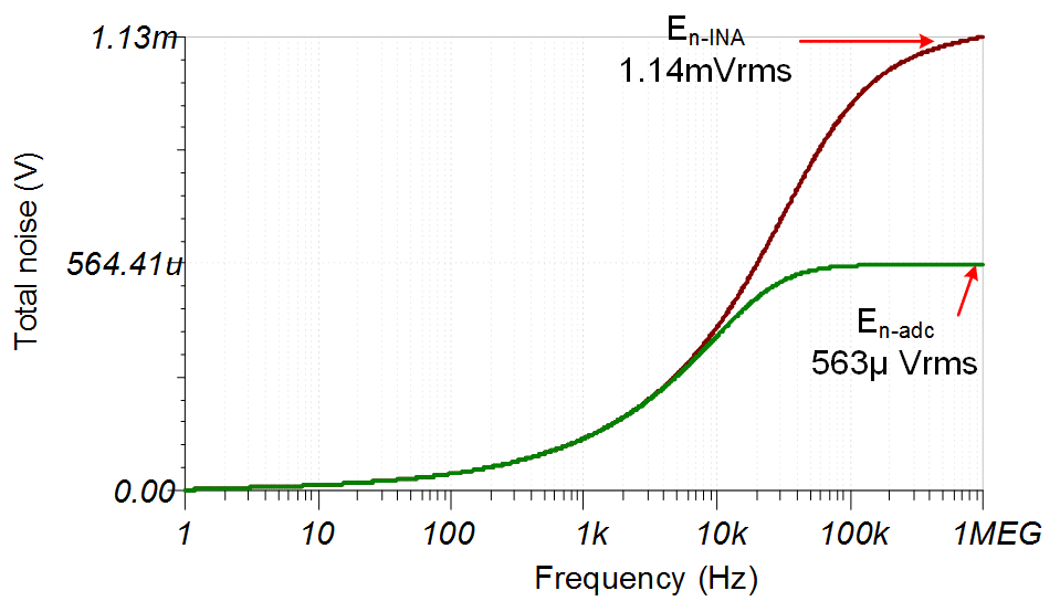
Noise Simulation
The section walks through a simplified noise calculation for a rough estimate. We neglect the noise from the OPA827 as the noise of the INA828 is dominant also neglect resistor noise in this calculation as it is attenuated for frequencies greater than 15.92kHz.
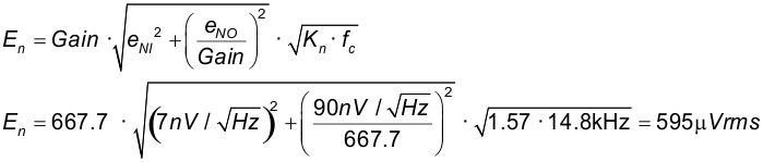
Note that calculated and simulated match well (simulated = 563µVRMS, calculated = 595µVRMS). See TI Precision Labs - Op Amps: Noise 4 for detailed theory on amplifier noise calculations and Calculating Total Noise for ADC Systems for data converter noise.
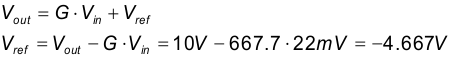
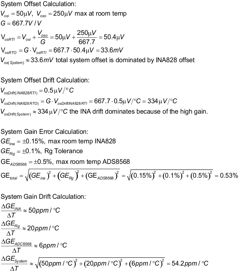
Gain Error and Offset Estimates
The following offset and offset drift calculations are dominated by the instrumentation amplifier since it is in high gain. Gain error calculations include the gain error of the ADC and instrumentation amplifier. For offset and gain error, the maximum room temperature value is used. See Statistics Behind Error Analysis for details on system gain and offset error.
Design Featured Devices
| Device | Key Features | Link | Other Possible Devices |
|---|---|---|---|
| ADS8568 | 16-bit resolution, SPI, 500kSPS sample rate, single-ended input, simultaneous sampling, internal reference, programmable range up to ±12V. | 16-bit, 8-channel, simultaneous-sampling, bipolar-input, SAR analog-to-digital converter (ADC) | Analog-to-digital converters (ADCs) |
| INA828 | Bandwidth 1MHz (G=1), low noise 18nV/√ Hz, low offset ±40μV, low offset drift ±0.4μV/°C, low gain drift 0.1ppm/°C (Typical values) | 50-μV Offset, 7-nV/√Hz Noise, Low-Power, Precision Instrumentation Amplifier | Instrumentation amplifiers |
| OPA827 | Gain bandwidth 22MHz, low noise 4nV/√ Hz, low offset ±75μV, low offset drift ±0.1μV/°C (Typical values) | Low-noise, high-precision, JFET-input operational amplifier | Operational amplifiers (op amps) |
Link to Key Files
Texas Instruments, SBAC215 source files, software support
Trademarks
All trademarks are the property of their respective owners.
IMPORTANT NOTICE AND DISCLAIMER
TI PROVIDES TECHNICAL AND RELIABILITY DATA (INCLUDING DATASHEETS), DESIGN RESOURCES (INCLUDING REFERENCE DESIGNS), APPLICATION OR OTHER DESIGN ADVICE, WEB TOOLS, SAFETY INFORMATION, AND OTHER RESOURCES “AS IS” AND WITH ALL FAULTS, AND DISCLAIMS ALL WARRANTIES, EXPRESS AND IMPLIED, INCLUDING WITHOUT LIMITATION ANY IMPLIED WARRANTIES OF MERCHANTABILITY, FITNESS FOR A PARTICULAR PURPOSE OR NON-INFRINGEMENT OF THIRD PARTY INTELLECTUAL PROPERTY RIGHTS.
These resources are intended for skilled developers designing with TI products. You are solely responsible for (1) selecting the appropriate TI products for your application, (2) designing, validating and testing your application, and (3) ensuring your application meets applicable standards, and any other safety, security, or other requirements. These resources are subject to change without notice. TI grants you permission to use these resources only for development of an application that uses the TI products described in the resource. Other reproduction and display of these resources is prohibited. No license is granted to any other TI intellectual property right or to any third party intellectual property right. TI disclaims responsibility for, and you will fully indemnify TI and its representatives against, any claims, damages, costs, losses, and liabilities arising out of your use of these resources.
TI’s products are provided subject to TI’s Terms of Sale (www.ti.com/legal/termsofsale.html) or other applicable terms available either on ti.com or provided in conjunction with such TI products. TI’s provision of these resources does not expand or otherwise alter TI’s applicable warranties or warranty disclaimers for TI products.
Mailing Address: Texas Instruments, Post Office Box 655303, Dallas, Texas 75265
Copyright © 2024, Texas Instruments Incorporated