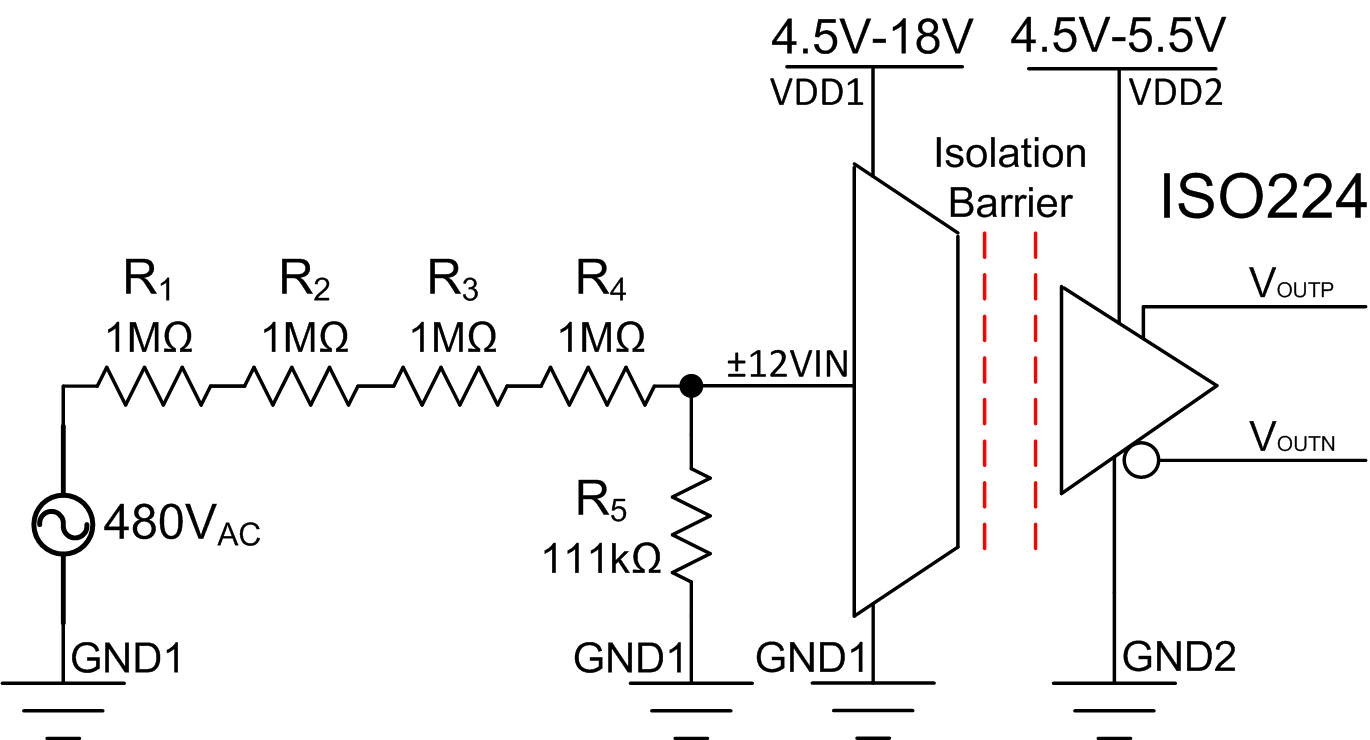
±480V Isolated Voltage-Sensing Circuit With Differential Output
Design Goals
| Voltage Source | ISO224 Input Voltage | ISO224 Output Voltage VDD2 / 2 Common Mode (VOUTP – VOUTN) | Power Supplies | ||||
|---|---|---|---|---|---|---|---|
| VMAX | VMIN | VIN, MAX | VIN, MIN | VOUT, MAX | VOUT, MIN | VDD1 | VDD2 |
| 480V | –480V | 12V | –12V | 4V | –4V | 4.5V–18V | 4.5V–5.5V |
Design Description
This circuit performs a ±480V, isolated, voltage-sensing measurement utilizing the ISO224 isolated amplifier and a voltage-divider circuit. The voltage-divider circuit reduces the voltage from ±480V to ±12V which matches the input range of the ISO224. The ISO224 is powered from both a high and low side power supply. Typically, the high side supply is generated using a floating supply or from the low side using an isolated transformer or isolated DC/DC converter. The ISO224 can measure single-ended signals of ±12V with a fixed gain of ⅓V/V and produces an isolated differential output voltage of ±4V with an output common-mode voltage of VDD2 / 2. The differential output voltage can be scaled as required using an additional operational amplifier such as the TLV6001 as shown in SBOA274 to interface with an ADC.
Design Notes
- Verify the systems linear operation for the desired input signal range. This is verified using simulation in the DC Transfer Characteristics section.
- Verify that the resistors used in the resistor divider circuit (R1–R5) are capable of dissipating the power supplied from the voltage source.
- Verify that the voltage on the input of the ISO224 is less than ±15V as stated in the absolute maximum ratings table of the data sheet and make sure that less than ±10mA is applied to the input. If the system is susceptible to transients, consider adding a TVS diode to the input. See the I-V Curve of the Input Clamp Protection Circuit image in the ISO224 Reinforced Isolated Amplifier with Single-Ended Input of ±12 V and Differential Output of ±4 V data sheet for additional details.
Design Steps
- Calculate the ratio from the voltage source to the input of the
ISO224 for the voltage-divider circuit.
- The typical input impedance of the ISO224 is 1.25MΩ. This
impedance is in parallel with resistor R5 and must be considered when
designing the voltage-divider circuit. Select 1MΩ resistors for R1,
R2, R3, and R4. Using the ratio from the
previous step and the following voltage-divider equation, solve for the
equivalent resistance required for the voltage-divider parallel combination ( ||
) of R5 and the ISO224 input impedance.
- Substituting 1.25MΩ for the ISO224 input impedance and using the
following equation, solve for R5. Use the analog
engineer's calculator to determine the closest standard value for
R5.
- Verify that the equivalent resistance is close to the
calculated resistance from step 2.
- Verify that the voltage-divider circuit is within a reasonable
error tolerance. For the following calculation, the input resistance of the
ISO224 is assumed to be the typical value of 1.25MΩ and this results in an error
of 0.6%. However, it is important to consider that the input resistance varies
from device to device due to variations in the resistance of the internal clamp
protection circuit. If the same calculation is performed using the minimum input
resistance of 1MΩ, the error is 2.5%. If this error range is unacceptable then
either a calibration must be performed or the resistance of the voltage-divider
circuit can be scaled down.
- Calculate the current flowing through the voltage-divider
circuit from the voltage source to make sure that the power dissipation does not
exceed the ratings of the resistor. For additional details, see Considerations for High Voltage Measurements.
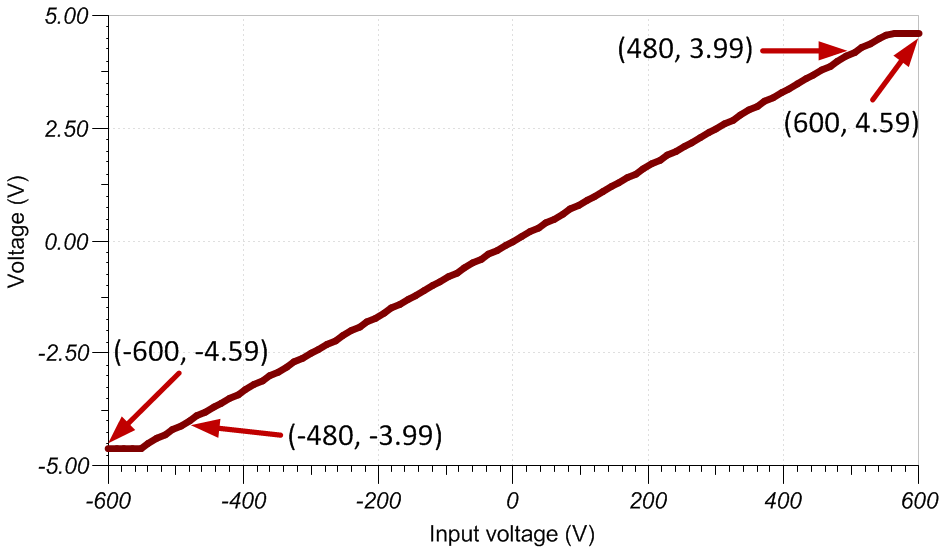
DC Transfer Characteristics
The following graph shows the simulated output for a ±600V input. The voltage divider scales the gain by 1/40, and the ISO224 scales the gain by an additional ⅓.
The transfer function shows the system gain is 1/40 from the voltage divider and ⅓ from the ISO224 (that is, gain × VIN = VOUT, (1/40) × (⅓) × (480V) = 4V).
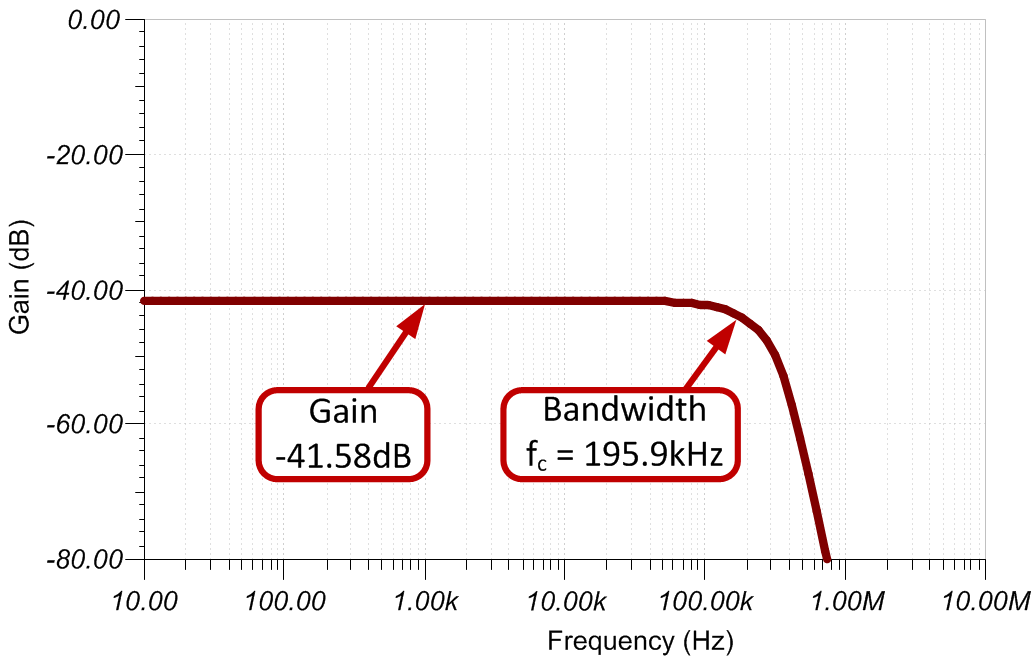
AC Transfer Characteristics
The simulated gain is –41.58dB (or 0.008337V/V) which closely matches the expected gain for the voltage divider and ISO224.
References
- Analog Engineer's Circuit Cookbooks
- SPICE Simulation File SBAC232
- TI Precision Designs TIDA-00835
- TI Precision Labs
Design Featured Isolated Op Amp
| ISO224B | |
|---|---|
| VDD1 | 4.5V–18V |
| VDD2 | 4.5V–5.5V |
| Input Voltage Range | ±12V |
| Nominal Gain | ⅓ |
| VOUT | Differential ±4V on output common mode of VDD2 / 2 |
| Input Resistance | 1.25MΩ (typ) |
| Small Signal Bandwidth | 275kHz |
| Input Offset Voltage and Drift | ±5mV (max), ±15µV/°C (max) |
| Gain Error and Drift | ±0.3% (max), ±35ppm/°C (max) |
| Nonlinearity and Drift | 0.01% (max), ±0.1ppm/°C (typ) |
| Isolation Transient Overvoltage | 7kVPEAK |
| Working Voltage | 1.5kVRMS |
| Common-mode transient immunity, CMTI | 55 kV/µs (min) |
| ISO224 | |
Design Alternate Isolated Op Amp
| AMC1311B | |
|---|---|
| VDD1 | 3V–5.5V |
| VDD2 | 3V–5.5V |
| Input Voltage range | 2V |
| Nominal Gain | 1 |
| VOUT | Differential ±2V on output common mode of 1.44V |
| Input Resistance | 1GΩ (typ) |
| Small Signal Bandwidth | 220kHz |
| Input Offset Voltage and Drift | ±1.5mV (max), ±15µV/°C (max) |
| Gain Error and Drift | ±0.3% (max), ±45ppm/°C (max) |
| Nonlinearity and Drift | 0.01%, 1ppm/°C (typ) |
| Isolation Transient Overvoltage | 7kVPEAK |
| Working Voltage | 1.5kVRMS |
| Common-mode transient immunity, CMTI | 75kV/µs (min) |
| AMC1311 | |
Trademarks
All trademarks are the property of their respective owners.
IMPORTANT NOTICE AND DISCLAIMER
TI PROVIDES TECHNICAL AND RELIABILITY DATA (INCLUDING DATASHEETS), DESIGN RESOURCES (INCLUDING REFERENCE DESIGNS), APPLICATION OR OTHER DESIGN ADVICE, WEB TOOLS, SAFETY INFORMATION, AND OTHER RESOURCES “AS IS” AND WITH ALL FAULTS, AND DISCLAIMS ALL WARRANTIES, EXPRESS AND IMPLIED, INCLUDING WITHOUT LIMITATION ANY IMPLIED WARRANTIES OF MERCHANTABILITY, FITNESS FOR A PARTICULAR PURPOSE OR NON-INFRINGEMENT OF THIRD PARTY INTELLECTUAL PROPERTY RIGHTS.
These resources are intended for skilled developers designing with TI products. You are solely responsible for (1) selecting the appropriate TI products for your application, (2) designing, validating and testing your application, and (3) ensuring your application meets applicable standards, and any other safety, security, or other requirements. These resources are subject to change without notice. TI grants you permission to use these resources only for development of an application that uses the TI products described in the resource. Other reproduction and display of these resources is prohibited. No license is granted to any other TI intellectual property right or to any third party intellectual property right. TI disclaims responsibility for, and you will fully indemnify TI and its representatives against, any claims, damages, costs, losses, and liabilities arising out of your use of these resources.
TI’s products are provided subject to TI’s Terms of Sale (www.ti.com/legal/termsofsale.html) or other applicable terms available either on ti.com or provided in conjunction with such TI products. TI’s provision of these resources does not expand or otherwise alter TI’s applicable warranties or warranty disclaimers for TI products.
Mailing Address: Texas Instruments, Post Office Box 655303, Dallas, Texas 75265
Copyright © 2024, Texas Instruments Incorporated