-
Multiple PCM6xx0 Devices With Shared TDM and I2C Bus SBAA415 April 2020 PCM6240-Q1 , PCM6260-Q1 , PCM6340-Q1 , PCM6360-Q1
-
Multiple PCM6xx0 Devices With Shared TDM and I2C Bus
Multiple PCM6xx0 Devices With Shared TDM and I2C Bus
Multiple PCM6xx0 Devices With Shared TDM and I2C Bus
The PCM6x40 device family (PCM6240 and PCM6340) is a quad-channel and the PCM6x60 device family (PCM6260 and PCM6360) is a six-channel, high-performance, analog-to-digital converter (ADC). This document describes how to configure multiple PCM6xx0 devices to share a single TDM and I2C Bus.
Trademarks
All other trademarks are the property of their respective owners.
1 Introduction
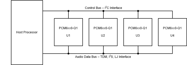
For PCM6xx0 applications requiring more than the channels supported by a single device, multiple PCM6xx0 devices can share a common bus. For systems with up to 16 analog input channels, up to four PCM6x40 devices can share a single control and audio data bus to minimize board routing area. For systems with up to 24 analog input channels, up to four PCM6x60 devices can share a single control and audio data bus to minimize board routing area. PCM6xx0 supports a control bus using the I2C interface and an audio serial bus using a time-division multiplexed (TDM), Inter-IC Sound (I2S), or Left-justified (LJ) interface. Figure 1 shows a diagram of four PCM6xx0 devices sharing the control and audio data buses.
 Figure 1. Four PCM6xx0 Devices With Shared Control and Audio Data Buses
 Each channel of the PCM6xx0 device follows the signal chain shown in Figure 2. Each channel of the PCM6xx0 supports an analog differential or single-ended signal. In PCM6xx0 device families, the analog input signal is amplified by a Programmable Gain Amplifier (PGA) and then converted by a high performance ADC into a digital signal. The PGA gains the input signal to match the full scale of the ADC. The digital signal has a programmable phase calibration to adjust the phase delay of each channel in steps of one modulator clock cycle. This allows the system to match the phase across different channels. The phase calibrated digital signal is then decimated through a set of linear phase filters or low latency filters. DC offset is removed from the decimated signal through a Digital High Pass Filter (HPF) with three pre-set cutoff frequencies or a fully programmable cutoff frequency. Note that DC shifts are caused by mismatches in common-mode voltages. The output of the HPF is gain calibrated with 0.1-dB steps and summed with other channels. The gain calibration matches the gain across different channels, particularly if the channels have microphones with varying gain values. The output is then filtered by the Digital Biquad Filters and gained by the volume control.
 Figure 2. PCM6xx0 Channel Signal Chain Processing Flow Chart
 This application note concentrates on how to configure the PCM6xx0 to share a single control and audio data bus between the devices.
2 Sharing the Control Bus
The PCM6xx0 devices are controlled through an I2C bus operating in standard mode, fast mode, and fast mode plus. This I2C control bus requires a 7-bit slave address whose two least significant bits are programmable by pulling the ADDR0_SCLK and ADDR1_MISO pins to VSS or IOVDD. By programming different I2C slave addresses through these pins, several PCM6xx0 devices can share a single I2C control bus. Moreover, a programmable broadcast enable feature allows you to temporarily change the I2C slave address to 1001000 for PCM6xx0. This temporary slave address allows for simultaneous broadcasting I2C communication to all PCM6xx0 devices in the system. Table 1 lists the four possible PCM6xx0 device addresses resulting from these pin and broadcast configuration options. In these table entries for ADDR1_MISO and ADDR0_SCLK, the notation '0' refers to pulling the pin to VSS, while notation '1' refers to pulling the pin to IOVDD. The notation 'X' refers to pulling the pin to either VSS or IOVDD.
Table 1. PCM6xx0 I2C Slave Address Settings
| ADDR1_MISO | ADDR0_SCLK | I2C_BRDCAST_EN Bit Field of SLEEP_CFG Register | I2C Slave Address (BINARY) |
|---|---|---|---|
| 0 | 0 | 0 (default) | 1001 000 |
| 0 | 1 | 0 (default) | 1001 001 |
| 1 | 0 | 0 (default) | 1001 010 |
| 1 | 1 | 0 (default) | 1001 011 |
| X | X | 1 | 1001 000 |