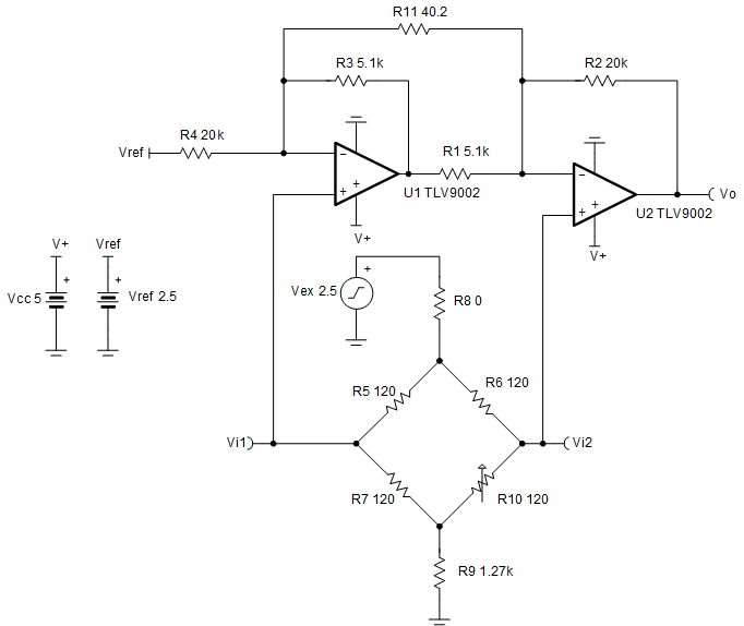
Single-Supply Strain Gauge Bridge Amplifier Circuit
Design Goals
| Input ViDiff(Vi2 – Vi1) | Output | Supply | ||||
|---|---|---|---|---|---|---|
| ViDiff_Min | ViDiff_Max | VoMin | VoMax | Vcc | Vee | Vref |
| –2.22 mV | 2.27 mV | 225 mV | 4.72 V | 5 V | 0 V | 2.5 V |
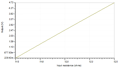
| Strain Gauge Resistance Variation (R10) | Vcm | Gain |
|---|---|---|
| 115 Ω – 125 Ω | 2.39 V | 1001 V/V |
Design Description
A strain gauge is a sensor whose resistance varies with applied force. The change in resistance is directly proportional to how much strain the sensor is experiencing due to the force applied. To measure the variation in resistance, the strain gauge is placed in a bridge configuration. This design uses a two op amp instrumentation circuit to amplify a differential signal created by the change in resistance of a strain gauge. By varying R10, a small differential voltage is created at the output of the Wheatstone bridge which is fed to the two op amp instrumentation amplifier input. Linear operation of an instrumentation amplifier depends upon the linear operation of the primary building block: op amps. An op amp operates linearly when the input and output signals are within the input common-mode and output-swing ranges of the device, respectively. The supply voltages used to power the op amps define these ranges.
Design Notes
- Resistors R5, R6, and R7 of the Wheatstone bridge must match the stain gauge nominal resistance and must be equal to avoid creating a bridge offset voltage.
- Low tolerance resistors must be used to minimize the offset and gain errors due to the bridge resistors.
- Vex sets the excitation voltage of the bridge and the common-mode voltage Vcm.
- Vref biases the output voltage of the instrumentation amplifier to mid-supply to allow differential measurements in the positive and negative directions.
- R11 sets the gain of the instrumentation amplifier circuit.
- R8 and R9 set the common-mode voltage of the instrumentation amplifier and limits the current through the bridge. This current determines the differential signal produced by the bridge. However, there are limitations on the current through the bridge due to self-heating effects of the bridge resistors and strain gauge.
- Make sure that R1 = R3 and R2 = R4 and that ratios of R2/R1 and R4/R3 are matched to set the Vref gain to 1 V/V and maintain high DC CMRR of the instrumentation amplifier.
- Linear operation is contingent upon the input common-mode and the output swing ranges of the op amps used. The linear output swing ranges are specified under the Aol test conditions in the op amps data sheets.
- Using high-value resistors can degrade the phase margin of the circuit and introduce additional noise in the circuit.
Design Steps
- Select R5, R6
and R7 to match the stain gauge nominal resistance
- Choose R9 to set the
common mode voltage of the instrumentation amplifier at 2.39 V
- Calculate the gain required to
produce the desired output voltage swing
- Select R1,
R2, R3, and R4. To set the Vref gain
at 1 V/V and avoid degrading the instrumentation amplifier’s CMRR, R1
must equal R3 and R2 must equal R4.
- Calculate R11 to meet
the required gain
- Calculate the current through the
bridge
Design Simulations
DC Simulation Results
References
- Analog Engineer's Circuit Cookbooks
- SPICE Simulation File SBOMAU4
- TI Precision Designs TIPD170
- TI Precision Labs
- VCM vs. VOUT plots for instrumentation amplifiers with two op amps
| TLV9002 | |
|---|---|
| Vss | 1.8 V to 5.5 V |
| VinCM | Rail-to-rail |
| Vout | Rail-to-Rail |
| Vos | 0.4 mV |
| Iq | 0.06 mA |
| Ib | 5 pA |
| UGBW | 1 MHz |
| SR | 2 V/µs |
| #Channels | 1, 2, and 4 |
| TLV9002 | |
Design Alternate Op Amp
| OPA376 | |
|---|---|
| Vss | 2.2 V to 5.5 V |
| VinCM | (Vee – 0.1 V) to (Vcc – 1.3 V) |
| Vout | Rail-to-Rail |
| Vos | 0.005 mV |
| Iq | 0.76 mA |
| Ib | 0.2 pA |
| UGBW | 5.5 MHz |
| SR | 2 V/µs |
| #Channels | 1, 2, and 4 |
| OPA376 | |
IMPORTANT NOTICE AND DISCLAIMER
TI PROVIDES TECHNICAL AND RELIABILITY DATA (INCLUDING DATASHEETS), DESIGN RESOURCES (INCLUDING REFERENCE DESIGNS), APPLICATION OR OTHER DESIGN ADVICE, WEB TOOLS, SAFETY INFORMATION, AND OTHER RESOURCES “AS IS” AND WITH ALL FAULTS, AND DISCLAIMS ALL WARRANTIES, EXPRESS AND IMPLIED, INCLUDING WITHOUT LIMITATION ANY IMPLIED WARRANTIES OF MERCHANTABILITY, FITNESS FOR A PARTICULAR PURPOSE OR NON-INFRINGEMENT OF THIRD PARTY INTELLECTUAL PROPERTY RIGHTS.
These resources are intended for skilled developers designing with TI products. You are solely responsible for (1) selecting the appropriate TI products for your application, (2) designing, validating and testing your application, and (3) ensuring your application meets applicable standards, and any other safety, security, or other requirements. These resources are subject to change without notice. TI grants you permission to use these resources only for development of an application that uses the TI products described in the resource. Other reproduction and display of these resources is prohibited. No license is granted to any other TI intellectual property right or to any third party intellectual property right. TI disclaims responsibility for, and you will fully indemnify TI and its representatives against, any claims, damages, costs, losses, and liabilities arising out of your use of these resources.
TI’s products are provided subject to TI’s Terms of Sale (www.ti.com/legal/termsofsale.html) or other applicable terms available either on ti.com or provided in conjunction with such TI products. TI’s provision of these resources does not expand or otherwise alter TI’s applicable warranties or warranty disclaimers for TI products.
Mailing Address: Texas Instruments, Post Office Box 655303, Dallas, Texas 75265
Copyright © 2023, Texas Instruments Incorporated