-
Enabling LVDS Links for Low Power FPGAs, Processors, and ASIC Implementations
Enabling LVDS Links for Low Power FPGAs, Processors, and ASIC Implementations
Low Voltage Differential Signaling (LVDS) has been the go to differential signaling standard for several decades. Since the inception of LVDS, electronic systems designers have turned to LVDS whenever the designers needed to implement high data rate, low power and noise tolerant data and control links. As systems designers leverage the latest processors, FPGA, and ASSP technologies, implementing low power and efficient LVDS links is more important than ever before. New processor technologies are being developed in smaller CMOS process geometries operating at much lower core voltages and as a result supporting the higher I/O (Input/Output) voltage levels of traditional LVDS receiver I/O (up to 3.3 V) can present design challenges. Other differential I/O standards such as PECL and CML also have similar interfacing challenges when being used with new lower power processor technologies. Increasing the overall power dissipation of a large processor or FPGA to support a few data inputs does not make sense for most applications.
System designers can use TI’s latest 1.8 V capable LVDS differential receiver to easily integrate LVDS links into their designs without having to sacrifice power or performance of their chosen processor. TI’s latest differential signal receiver can help systems designers easily integrate differential signals such as LVDS, LVPECL, and CML into their lower power processor’s single ended inputs that operate at 1.8 V (see Figure 1 for an example use case). The new DS90LVRA2 is a two-channel LVDS (differential) receiver supporting single ended 1.8 V CMOS outputs that can easily be interfaced with 1.8 V inputs commonly found on most processors, FPGAs and ASSP devices.
 Figure 1 Example of DS90LVRA2 Use Case
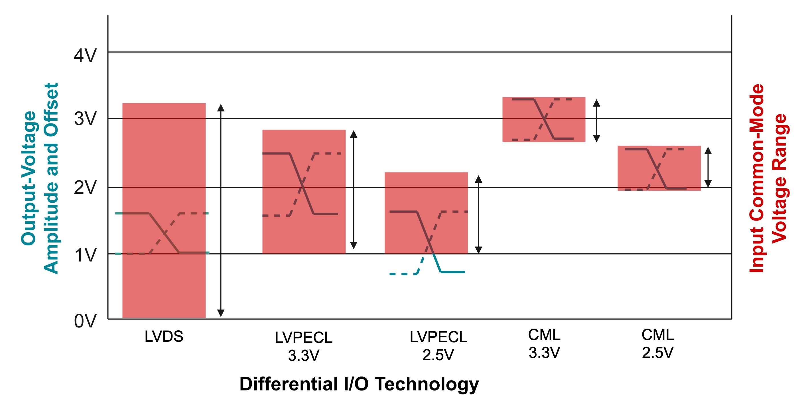
The DS90LVRA2 supports two differential input channels and two single-ended 1.8 V CMOS output channels operating up to 600 Mbps (300 MHz) for each differential input. The device has flexible inputs capable of accepting LVDS, LVPECL, or CML differential inputs (see Figure 2), requires a single voltage supply (1.8 V) and is housed in an eight pin WSON package supporting a flow through pinout. Higher data rate differential signals like LVDS and LVPECL need to be properly terminated to avoid impairing signal integrity therefore discrete methods of level shifting and conversion are not recommended. Using the DS90LVRA2 results in superior signal performance compared to discrete level shifting implementations especially for higher data rates where discrete devices like amplifiers and resistors can actually degrade signal performance while also increasing cost and component count. For more information on the DS90LVRA2 please visit the DS90LVRA2 devices product page on ti.com. The device is also available in an automotive grade option, the DS90LVRA2-Q1.
 Figure 2 Differential Signaling Standard Inputs Supported by DS90LVRA2 LVDS, CML, LVPECL
IMPORTANT NOTICE AND DISCLAIMER
TI PROVIDES TECHNICAL AND RELIABILITY DATA (INCLUDING DATASHEETS), DESIGN RESOURCES (INCLUDING REFERENCE DESIGNS), APPLICATION OR OTHER DESIGN ADVICE, WEB TOOLS, SAFETY INFORMATION, AND OTHER RESOURCES “AS IS” AND WITH ALL FAULTS, AND DISCLAIMS ALL WARRANTIES, EXPRESS AND IMPLIED, INCLUDING WITHOUT LIMITATION ANY IMPLIED WARRANTIES OF MERCHANTABILITY, FITNESS FOR A PARTICULAR PURPOSE OR NON-INFRINGEMENT OF THIRD PARTY INTELLECTUAL PROPERTY RIGHTS.
These resources are intended for skilled developers designing with TI products. You are solely responsible for (1) selecting the appropriate TI products for your application, (2) designing, validating and testing your application, and (3) ensuring your application meets applicable standards, and any other safety, security, or other requirements. These resources are subject to change without notice. TI grants you permission to use these resources only for development of an application that uses the TI products described in the resource. Other reproduction and display of these resources is prohibited. No license is granted to any other TI intellectual property right or to any third party intellectual property right. TI disclaims responsibility for, and you will fully indemnify TI and its representatives against, any claims, damages, costs, losses, and liabilities arising out of your use of these resources.
TI’s products are provided subject to TI’s Terms of Sale (www.ti.com/legal/termsofsale.html) or other applicable terms available either on ti.com or provided in conjunction with such TI products. TI’s provision of these resources does not expand or otherwise alter TI’s applicable warranties or warranty disclaimers for TI products.
Mailing Address: Texas Instruments, Post Office Box 655303, Dallas, Texas 75265
Copyright © 2024, Texas Instruments Incorporated