-
Enabling AI Accelerators with Voltage Level Translation SCEA141 May 2024 LSF0102 , PCA9306 , SN74AXC8T245 , TXU0304 , TXV0106 , TXV0106-Q1 , TXV0108 , TXV0108-Q1
-
Enabling AI Accelerators with Voltage Level Translation
Enabling AI Accelerators with Voltage Level Translation
Several of today’s electronic end equipment applications are adding artificial intelligence (AI) capabilities to help bring new functionality and user experiences to end applications enabling users to harness the power of AI in their day to day work flows. To bring AI capabilities to their end application, electronic system designers need to leverage large language models (LLM) such as Generative Pre-trained Transformers (GPT) which requires high performance compute capabilities on both the cloud side as well as the client side of applications. Enabling AI capabilities on device or by leveraging cloud-based compute infrastructure requires client systems and cloud infrastructure designers to leverage the latest processor technologies.
GPT based AI implementations require system designers to not only use the latest high-performance processors and FPGAs (CPU based devices) but also use the latest high-performance GPU (Graphic Processing Units) that are better suited for AI given their ability to parallel process large amounts of data as well as higher memory bandwidths needed for high speed data transfer. Using the latest CPUs and GPUs to support AI functionality does present systems designer with multiple design challenges.
One of these design challenges is overcoming the control and low speed data I/O level mismatches that results from operating CPUs and GPUs at very low core voltages. Operating high performance CPUs and GPUs at low core voltages is often an absolute requirement for achieving target performance levels given the thermal and power limitations of a specific processor. Operating CPUs and GPUs at low core voltages limits the I/O voltage levels that these processors can support.
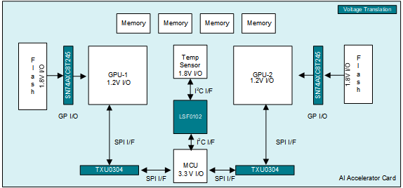
System designers often need a simple, efficient and scalable way to connect the numerous I/O and control buses of their GPU processors to peripheral devices and sub-systems. One design approach that enables system designers to maintain the CPU’s or GPU’s lower core voltage and still resolve I/O level mismatches is to use simple voltage level translator devices. Level translation devices provide system designers an easy and cost-effective solution for resolving their system’s I/O level mismatch challenges without having to compromise on performance, power, or size. See Figure 1.
 Figure 1 AI
Accelerator Card Block Diagram
Figure 1 AI
Accelerator Card Block DiagramIntegrated level shifting designs are available in a wide assortment of I/O types, bit widths, data rate ranges, current drive capabilities, and package options. Texas Instruments’ portfolio of level shifter devices contains many different types of level translation functions that collectively is able to address almost any interface requirement likely needed for high performance compute use cases for AI applications. TI’s level translation portfolio includes Auto Directional, Direction Controlled, and Fixed Direction level translators in Industrial, Automotive and Enhanced ratings. Table 1 shows common control interfaces found on high-performance CPU and GPU families and recommended level translation devices for each interface supporting voltage ranges from < 0.8 V to 5.5 V. For more information on all of TI’s level translation devices, please visit TI’s Level Translation Landing Page.
| Translation Level | ||
|---|---|---|
| Interface | Up to 3.6V | Up to 5.5V |
| FET Replacement | 2N7001T | SN74LXC1T45/TXU0101 |
| 1 Bit GPIO/Clock Signal | SN74AXC1T45 | SN74LXC1T45/TXU0101 |
| 2 Bit GPIO | SN74AXC2T245 | SN74LXC2T45 / TXU0x02 |
| 2-Pin JTAG/UART | SN74AXC2T45 | SN74LXC2T45 / TXU0x02 |
| I2C/MDIO/SMBus | TXS0102 / LSF0102 / PCA9306 | TXS0102 / LSF0102 / PCA9306 |
| I3C | TCA39306 | |
| 4 Bit GPIO | SN74AXC4T245 | TXB0104 / TXU0104 |
| UART | SN74AXC4T245 | TXB0104 / TXU0204 |
| SPI | SN74AXC4T774 / TXB0104 | TXB0104 / TXU0304 |
| JTAG | SN74AXC4T774/ TXB0104 | TXB0104 / TXU0204 |
| I2S/PCM | SN74AXC4T774 / TXB0104 | TXB0104 / TXU0204 |
| Quad-SPI | TXB0106 | TXB0106 |
| SDIO/SD/MMC | TXS0206 / TWL1200 | NA |
| 8 Bit GPIO/RGMII | TXV0106/TXV0108 | SN74LXC8T245 |
IMPORTANT NOTICE AND DISCLAIMER
TI PROVIDES TECHNICAL AND RELIABILITY DATA (INCLUDING DATASHEETS), DESIGN RESOURCES (INCLUDING REFERENCE DESIGNS), APPLICATION OR OTHER DESIGN ADVICE, WEB TOOLS, SAFETY INFORMATION, AND OTHER RESOURCES “AS IS” AND WITH ALL FAULTS, AND DISCLAIMS ALL WARRANTIES, EXPRESS AND IMPLIED, INCLUDING WITHOUT LIMITATION ANY IMPLIED WARRANTIES OF MERCHANTABILITY, FITNESS FOR A PARTICULAR PURPOSE OR NON-INFRINGEMENT OF THIRD PARTY INTELLECTUAL PROPERTY RIGHTS.
These resources are intended for skilled developers designing with TI products. You are solely responsible for (1) selecting the appropriate TI products for your application, (2) designing, validating and testing your application, and (3) ensuring your application meets applicable standards, and any other safety, security, or other requirements. These resources are subject to change without notice. TI grants you permission to use these resources only for development of an application that uses the TI products described in the resource. Other reproduction and display of these resources is prohibited. No license is granted to any other TI intellectual property right or to any third party intellectual property right. TI disclaims responsibility for, and you will fully indemnify TI and its representatives against, any claims, damages, costs, losses, and liabilities arising out of your use of these resources.
TI’s products are provided subject to TI’s Terms of Sale (www.ti.com/legal/termsofsale.html) or other applicable terms available either on ti.com or provided in conjunction with such TI products. TI’s provision of these resources does not expand or otherwise alter TI’s applicable warranties or warranty disclaimers for TI products.
Mailing Address: Texas Instruments, Post Office Box 655303, Dallas, Texas 75265
Copyright © 2024, Texas Instruments Incorporated