-
Configurable Delay Blocks in TI's Programmable Logic Devices
Configurable Delay Blocks in TI's Programmable Logic Devices
1
Application Description
Delaying a signal is an important function in many analog and logic systems, and TI Programmable Logic Devices (TPLD) offer multiple blocks that can delay both signals generated inside the device and signals from an external source. Each block behaves differently and, while there are many simple delay applications where any block can be used, understanding the differences of the blocks allows a designer to optimize their system. This document will cover the delay blocks present in TPLD1201, TPLD1202, and TPLD801, how each block is configured in InterConnect Studio (ICS), and applications specific to each delay block.
Delay Blocks
The basic delay block accepts an input signal and delays that signal for a number of clock pulses configured using the Control Data setting, which can be set from 1 to 255.
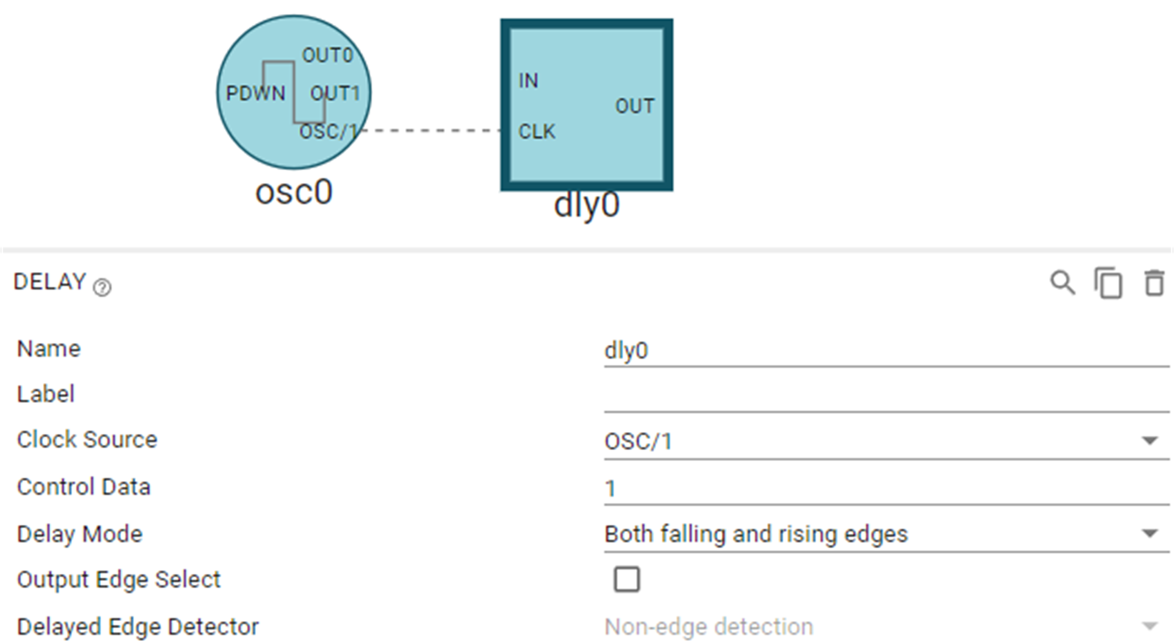 Figure 1 Delay Block in ICS
The clock can be set using the internal oscillators of the device, the internal oscillators modified by a frequency divider, or an external clock signal.
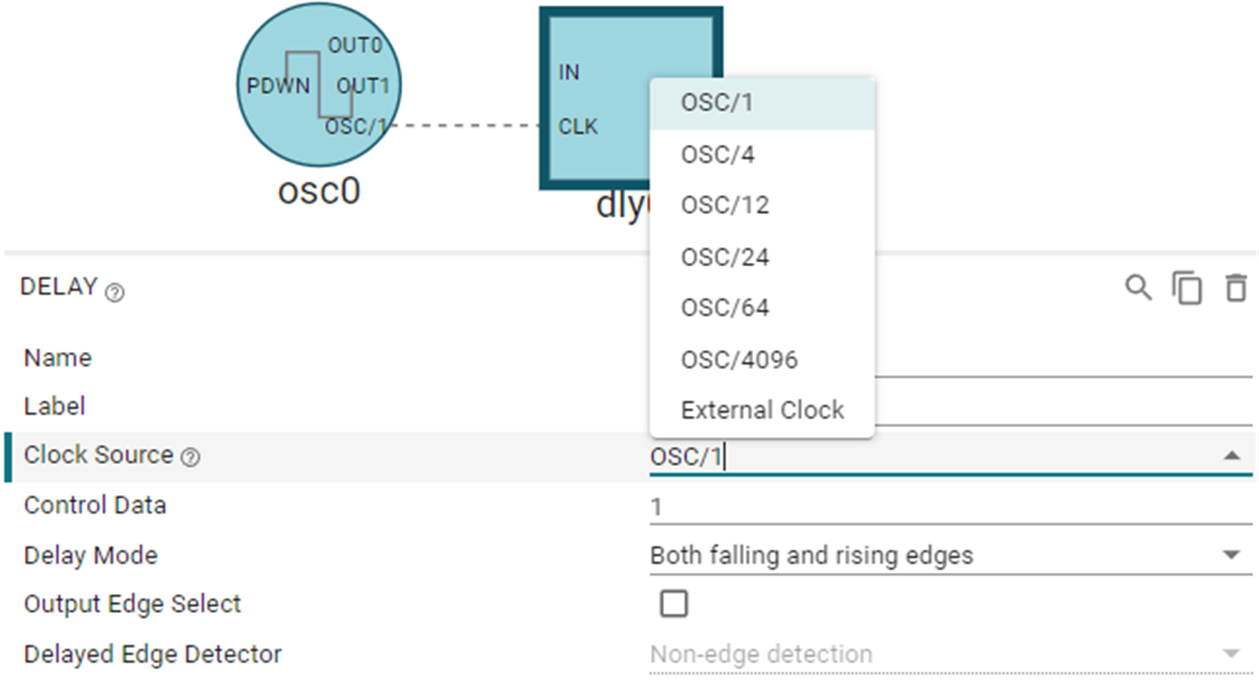 Figure 2 Frequency Divider
The designer can also select which edge to delay using the Delay Mode setting. Any edge not set to delay is passed through when detected, as shown in Figure 3 with a signal set to rising edge delay only.
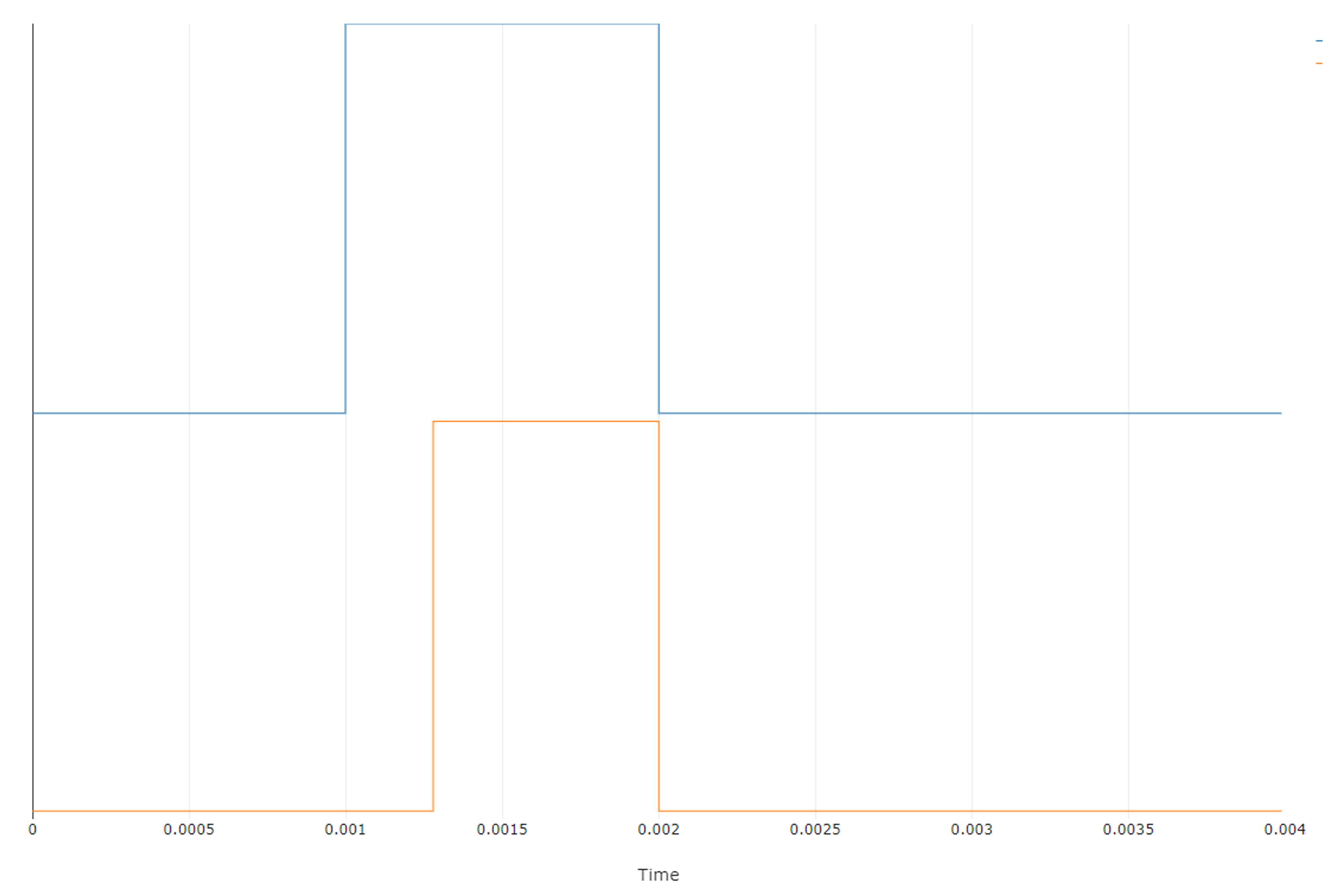 Figure 3 Rising Edge Only Delay ICS Simulation
The delay block is versatile and can be used to generate long delays by setting a high control data with low frequency clock source. This is shown in the voltage monitor design shown in Figure 4. In this design, the delay block sets a limit equal to the delay to the pulse length that can be sent when the analog comparator sends a high signal. The delay is set to use the 25kHz counter with a control data of 125, for a total delay of 5 ms.
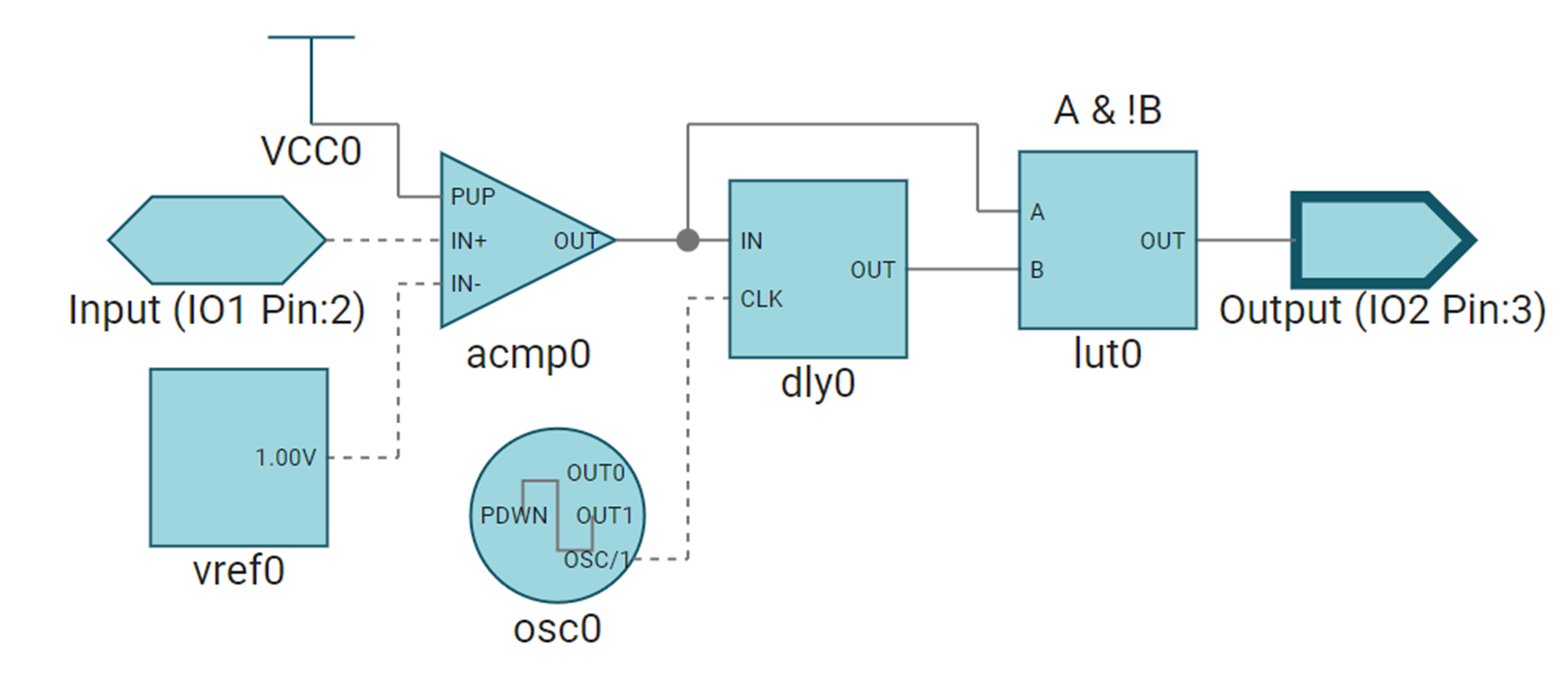 Figure 4 Voltage Monitor in ICS
Pipe Delay, Shift Register Blocks
The pipe delay, shift register block acts as a series of flip flops, and allows the user to set the number of flip flops in the sequence. The pipe delay block and shift register block both allow for up to 8 flip flops to be set in series.
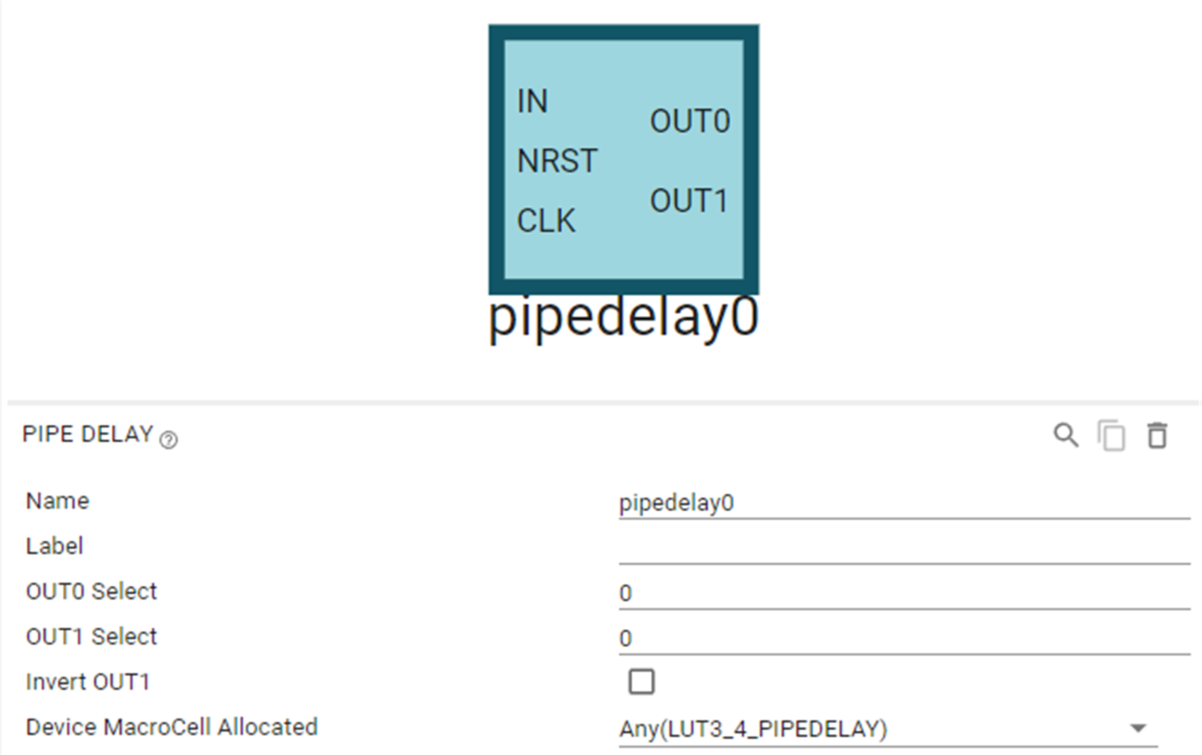 Figure 5 Pipe Delay Block
The key distinction between the pipe delay block and the shift register block is that the pipe delay block allows for two outputs from the sequence of flip flops, while the shift register block allows only one. However, the shift register block allows for additional control over the flip flops, with set or reset functionality and control over the initial state of the flip flops.
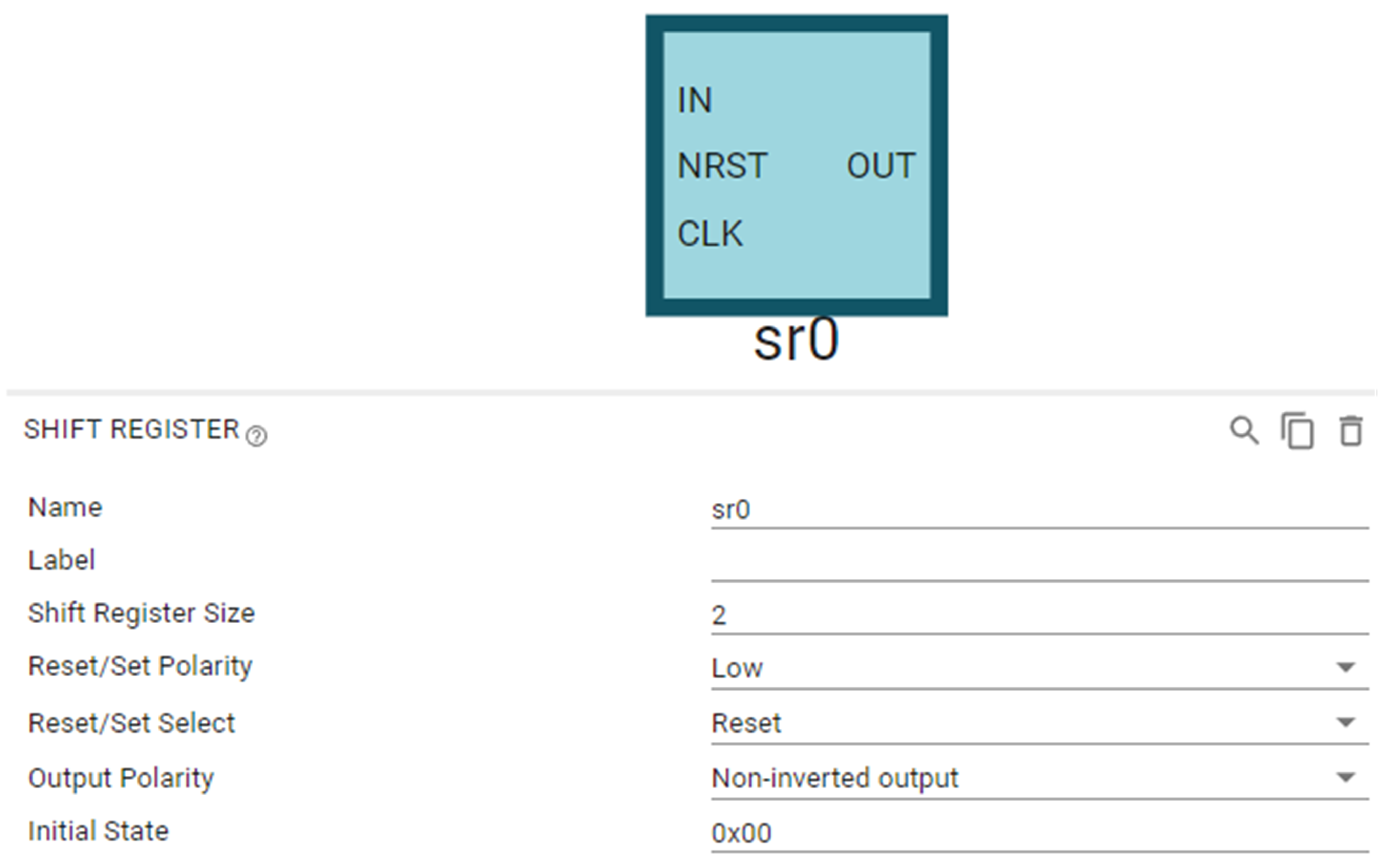 Figure 6 Shift Register Block
The pipe delay and shift register blocks are useful when sampling inputs or whenever a shift register is needed. In this example, a shift register is used to sample an input PWM signal, and the sampled signal is sent as an output when a reset signal is sent.
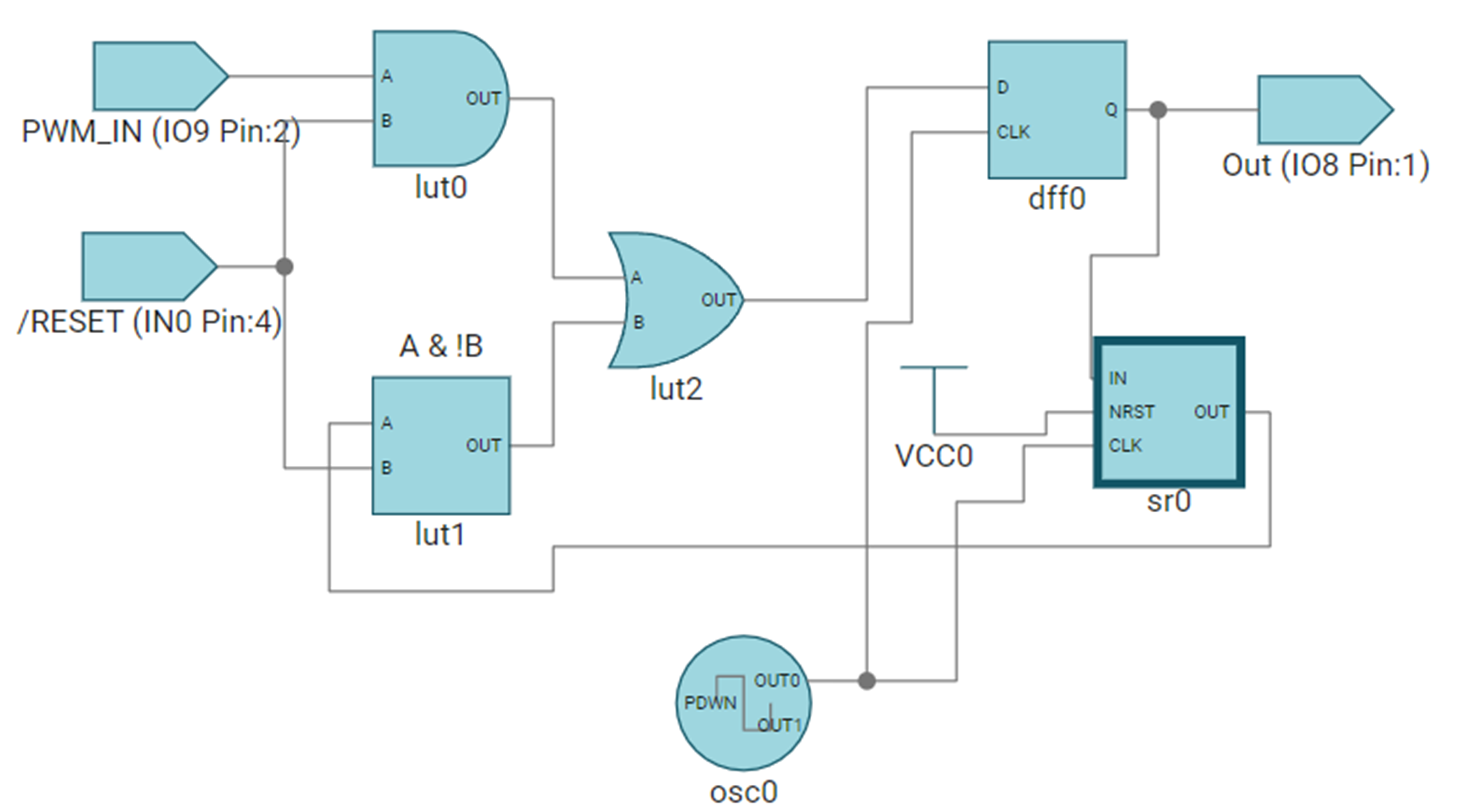 Figure 7 PWM Sampler in ICS
Programmable Filter Blocks
The programmable filter block typically acts as an edge detector. However, the programmable filter block has a delay mode that can be selected in ICS.
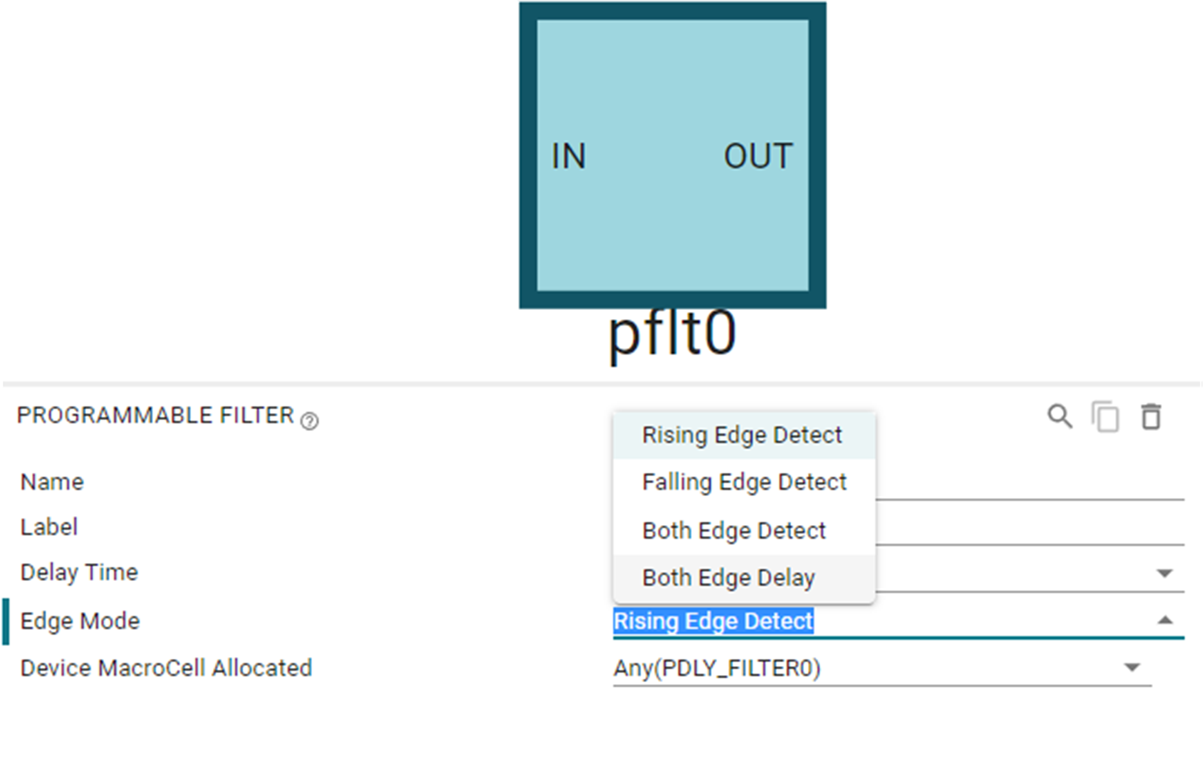 Figure 8 Programmable Filter in
ICS
Figure 8 Programmable Filter in
ICSWhen in delay mode, the programmable filter block delays the input signal by the selected delay time, filtering out any signals shorter than the delay time in the process. Unlike the other delay blocks, which are controlled by a clock signal, the programmable filter has a selection of pre-configured delay times that are not controlled by an oscillator.
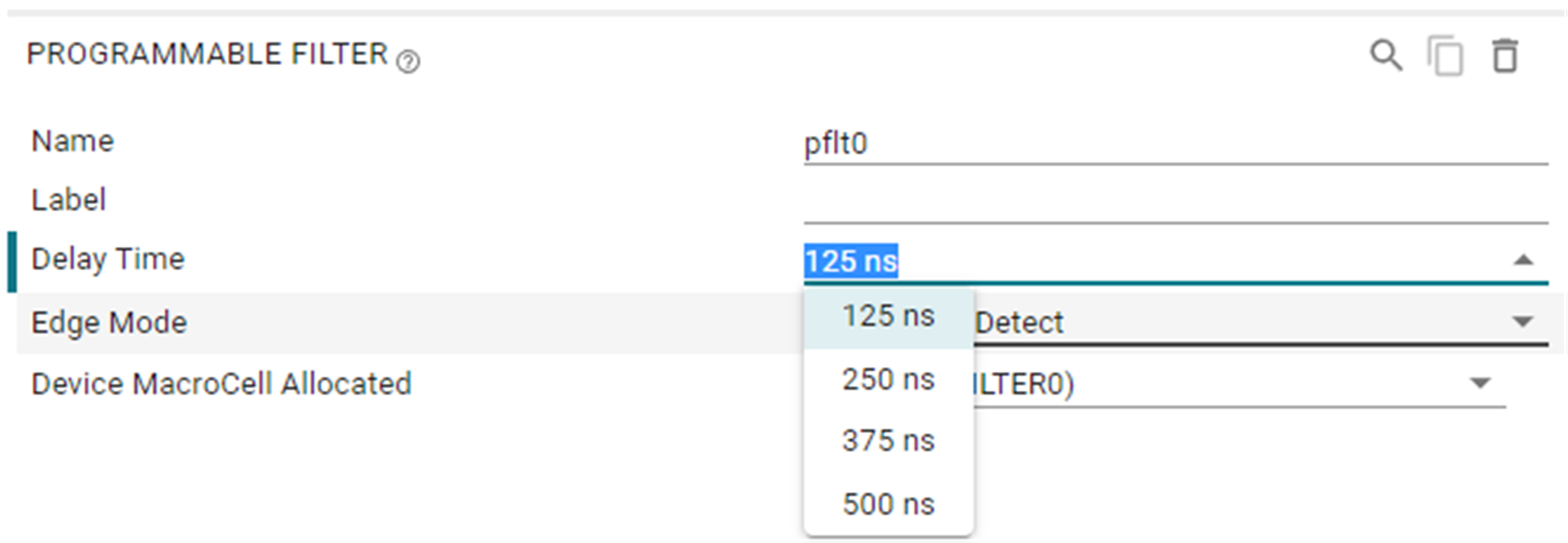 Figure 9 Programmable Filter Delay Times
This allows a designer to set a smaller delay than can be possible with an oscillator-controlled delay. The delay can also be more consistent than an oscillator-controlled delay block. In this example, the block is used to delay a signal by 125ns, with an additional delay caused by propagation of the signal through the device. With a regular delay block operating at maximum oscillator speed on the TPLD1201, the minimum delay possible is 500ns.
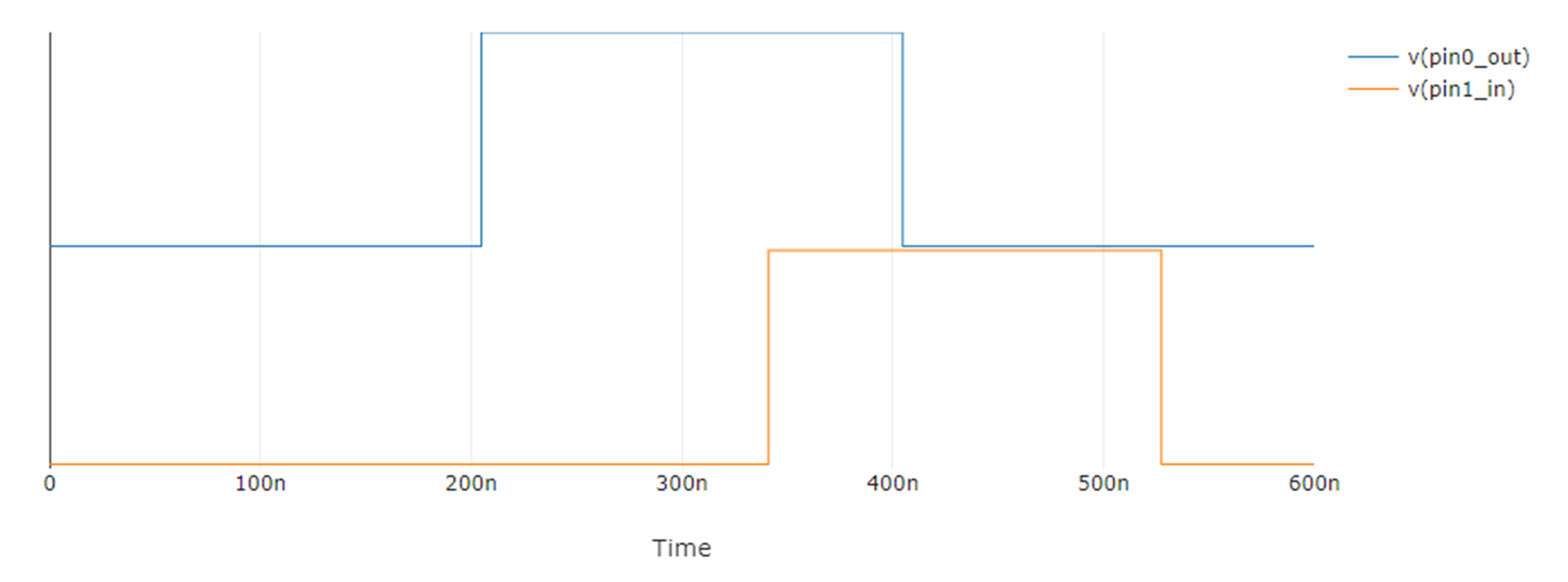 Figure 10 Programmable Filter ICS Simulation
Conclusions
Delaying a signal is a basic function of signal handling that can be implemented with several different methods, each with different optimizations. By integrating several different signal delay methods into a single device, TPLD gives designers more flexibility in their designs without increasing the BOM or board size.
Learn more about TI’s portfolio of programmable logic devices
Trademarks
All trademarks are the property of their respective owners.
IMPORTANT NOTICE AND DISCLAIMER
TI PROVIDES TECHNICAL AND RELIABILITY DATA (INCLUDING DATASHEETS), DESIGN RESOURCES (INCLUDING REFERENCE DESIGNS), APPLICATION OR OTHER DESIGN ADVICE, WEB TOOLS, SAFETY INFORMATION, AND OTHER RESOURCES “AS IS” AND WITH ALL FAULTS, AND DISCLAIMS ALL WARRANTIES, EXPRESS AND IMPLIED, INCLUDING WITHOUT LIMITATION ANY IMPLIED WARRANTIES OF MERCHANTABILITY, FITNESS FOR A PARTICULAR PURPOSE OR NON-INFRINGEMENT OF THIRD PARTY INTELLECTUAL PROPERTY RIGHTS.
These resources are intended for skilled developers designing with TI products. You are solely responsible for (1) selecting the appropriate TI products for your application, (2) designing, validating and testing your application, and (3) ensuring your application meets applicable standards, and any other safety, security, or other requirements. These resources are subject to change without notice. TI grants you permission to use these resources only for development of an application that uses the TI products described in the resource. Other reproduction and display of these resources is prohibited. No license is granted to any other TI intellectual property right or to any third party intellectual property right. TI disclaims responsibility for, and you will fully indemnify TI and its representatives against, any claims, damages, costs, losses, and liabilities arising out of your use of these resources.
TI’s products are provided subject to TI’s Terms of Sale (www.ti.com/legal/termsofsale.html) or other applicable terms available either on ti.com or provided in conjunction with such TI products. TI’s provision of these resources does not expand or otherwise alter TI’s applicable warranties or warranty disclaimers for TI products.
Mailing Address: Texas Instruments, Post Office Box 655303, Dallas, Texas 75265
Copyright © 2024, Texas Instruments Incorporated