-
TAS5756M Digital Input, Closed-Loop Class-D Amplifier With Processing
- 1 Features
- 2 Applications
- 3 Description
- 4 Revision History
- 5 Device Comparison Table
- 6 Pin Configuration and Functions
-
7 Specifications
- 7.1 Absolute Maximum Ratings
- 7.2 ESD Ratings
- 7.3 Recommended Operating Conditions
- 7.4 Thermal Information
- 7.5 Electrical Characteristics
- 7.6 MCLK Timing
- 7.7 Serial Audio Port Timing - Slave Mode
- 7.8 Serial Audio Port Timing - Master Mode
- 7.9 I2C Bus Timing - Standard
- 7.10 I2C Bus Timing - Fast
- 7.11 SPK_MUTE Timing
- 7.12 Power Dissipation
- 7.13 Typical Characteristics
-
8 Detailed Description
- 8.1 Overview
- 8.2 Functional Block Diagram
- 8.3
Feature Description
- 8.3.1 Power-on-Reset (POR) Function
- 8.3.2 Device Clocking
- 8.3.3
Serial Audio Port
- 8.3.3.1 Clock Master Mode from Audio Rate Master Clock
- 8.3.3.2 Clock Master from a Non-Audio Rate Master Clock
- 8.3.3.3 Clock Slave Mode with 4-Wire Operation (SCLK, MCLK, LRCK/FS, SDIN)
- 8.3.3.4 Clock Slave Mode with SLCK PLL to Generate Internal Clocks (3-Wire PCM)
- 8.3.3.5 Serial Audio Port - Data Formats and Bit Depths
- 8.3.3.6 Input Signal Sensing (Power-Save Mode)
- 8.3.3.7 Serial Data Output
- 8.3.4 Modulation Scheme
- 8.3.5 miniDSP Audio Processing Engine
- 8.3.6 Adjustable Amplifier Gain and Switching Frequency Selection
- 8.3.7
Error Handling and Protection Suite
- 8.3.7.1 Device Overtemperature Protection
- 8.3.7.2 SPK_OUTxx Overcurrent Protection
- 8.3.7.3 DC Offset Protection
- 8.3.7.4 Internal VAVDD Undervoltage-Error Protection
- 8.3.7.5 Internal VPVDD Undervoltage-Error Protection
- 8.3.7.6 Internal VPVDD Overvoltage-Error Protection
- 8.3.7.7 External Undervoltage-Error Protection
- 8.3.7.8 Internal Clock Error Notification (CLKE)
- 8.3.8 GPIO Port and Hardware Control Pins
- 8.3.9 I2C Communication Port
- 8.4 Device Functional Modes
-
9 Application and Implementation
- 9.1 Application Information
- 9.2
Typical Applications
- 9.2.1 2.0 (Stereo BTL) System
- 9.2.2 Mono (PBTL) Systems
- 9.2.3 2.1 (Stereo BTL + External Mono Amplifier) Systems
- 9.2.4 2.2 (Dual Stereo BTL) Systems
- 9.2.5 1.1 (Dual BTL, Bi-Amped) Systems
- 10Power Supply Recommendations
- 11Layout
- 12Device and Documentation Support
- 13Mechanical, Packaging, and Orderable Information
- IMPORTANT NOTICE
TAS5756M Digital Input, Closed-Loop Class-D Amplifier With Processing
1 Features
- Flexible Audio I/O Configuration
- Supports I2S, TDM, LJ, RJ Digital Input
- 8 kHz to 192 kHz Sample Rate Support
- Stereo Bridge Tied Load (BTL) or Mono Parallel Bridge Tied Load (PBTL) Operation
- BD Amplifier Modulation
- Supports 3-Wire Digital Audio Interface (No MCLK required)
- High-Performance Closed-Loop Architecture (PVDD = 12V, RSPK = 8 Ω, SPK_GAIN = 20 dBV)
- Idle Channel Noise = 56 µVrms (A-Wtd)
- THD+N = 0.006 % (at 1 W, 1 kHz)
- SNR = 104 A-Wtd (Ref. to THD+N = 1%)
-
PurePath™ HybridFlow Processing Architecture
- Several Configurable MiniDSP Programs (called HybridFlows)
- Download Time <100 ms (typ)
- Advanced Audio Processing Algorithms (2)
- Communication Features
- Software Mode Control via I2C Port
- Two Address Select Pins – Up to 4 Devices
- Robustness and Reliability Features
- Clock Error, DC, and Short-Circuit Protection
- Over Temperature and Overcurrent Protection
2 Applications
- LCD, LED TV, and Multi-Purpose Monitors
- Sound Bars, Docking Stations, PC Audio
- Wireless Subwoofers, Bluetooth and Active Speakers
3 Description
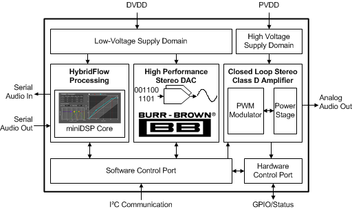
The TAS5756M device is a high-performance, stereo closed-loop amplifier with integrated audio processor with architecture. To convert from digital to analog, the device uses a high performance DAC with Burr-Brown® mixed signal heritage. It requires only two power supplies; one DVDD for low-voltage circuitry and one PVDD for high-voltage circuitry. It is controlled by a software control port using standard I2C communication. In the family, the TAS5756M uses traditional BD modulation, ensuring low distortion characteristics. The TAS5754M uses 1SPW modulation to reduce output ripple current, the expense of slightly higher distortion.
The unique HybridFlow architecture allows the system designer to choose from several configurable DSP programs that are specifically designed for use in popular audio end equipment such as bluetooth (BT) speakers, sound bars, docking stations, and subwoofers. This architecture combines the flexibility of a fully programmable device with the fast download time and ease of use of a fixed-function ROM device.
An optimal mix of thermal performance and device cost is provided in the 90 mΩ rDS(on) of the output MOSFETs. Additionally, a thermally enhanced 48-Pin HTSSOP provides excellent operation in the elevated ambient temperatures found in modern consumer electronic devices.
Device Information(1)
| PART NUMBER | PACKAGE | BODY SIZE (NOM) |
|---|---|---|
| TAS5756M | HTSSOP (48) | 12.50 mm × 6.10 mm |
- For all available packages, see the orderable addendum at the end of the datasheet.
- Please refer to SLAU577 for information regarding Audio Processing options available via the HybridFlow library.
- Tested on TAS5756MDCAEVM.
Simplified Block Diagram
Power at 10% THD+N vs PVDD(3)
4 Revision History
Changes from A Revision (January 2015) to B Revision
- Added TAS880021DCA device to Device Comparison TableGo
- Clarified OCECLRTIME specification in Electrical Characteristics tableGo
- Clarified OTECLRTIME specification in Electrical Characteristics tableGo
- Corrected several typographical errors in Electrical Characteristics tableGo
- Removed reference to Frequency Response graphs in Table 1Go
- Clarified clock generation explanation in Device Clocking sectionGo
- Clarified description of the modulation scheme used in the Class D amplifier in Modulation Scheme sectionGo
- Added clarity to Adjustable Amplifier Gain and Switching Frequency Selection sectionGo
- Added example resistor values for SPK_GAIN/FREQ pin configuration to Table 15Go
- Clarified the description of overtemperature error from latching to self-clearing in Device Overtemperature Protection sectionGo
- Corrected description of the overcurrent protection error from latching to self-clearing in SPK_OUTxx Overcurrent Protection sectionGo
- Added clarity to I2C Communication Port sectionGo
- Added Programming the TAS5756M sectionGo
- Updated Table 22Go
- Updated Table 25Go
- Updated Table 27Go
Changes from * Revision (June 2014) to A Revision
- Corrected typographical error in Device Information table Go
- Updated Functional Block DiagramGo
- Updated Table 15Go
- Added component specification note in Application and Implementation sectionGo
5 Device Comparison Table
6 Pin Configuration and Functions

Pin Functions
| PIN | TYPE(1) | INTERNAL TERMINATION | DESCRIPTION | |
|---|---|---|---|---|
| NAME | NO. | |||
| ADR0 | 26 | DI | Figure 11 | Sets the LSB of the I2C address to 0 if pulled to GND, to 1 if pulled to DVDD |
| ADR1 | 20 | DI | Sets the second LSB of the I2C address to 0 if pulled to GND, to 1 if pulled to DVDD | |
| AGND | 10 | G | — | Ground reference for analog circuitry(2) |
| 15 | ||||
| AVDD | 14 | P | Figure 2 | Power supply for internal analog circuitry |
| BSTRPA– | 1 | P | Figure 3 | Connection point for the SPK_OUTA– bootstrap capacitor which is used to create a power supply for the high-side gate drive for SPK_OUTA– |
| BSTRPA+ | 5 | P | Connection point for the SPK_OUTA+ bootstrap capacitor which is used to create a power supply for the high-side gate drive for SPK_OUTA | |
| BSTRPB– | 48 | P | Connection point for the SPK_OUTB– bootstrap capacitor which is used to create a power supply for the high-side gate drive for SPK_OUTB– | |
| BSTRPB+ | 44 | P | Connection point for the SPK_OUTB+ bootstrap capacitor which is used to create a power supply for the high-side gate drive for SPK_OUTB+ | |
| CN | 34 | P | Figure 15 | Negative pin for capacitor connection used in the line--driver charge pump |
| CP | 32 | P | Figure 14 | Positive pin for capacitor connection used in the line-driver charge pump |
| CPVDD | 31 | P | Figure 2 | Power supply for charge pump circuitry |
| CPVSS | 35 | P | Figure 15 | –3.3-V supply generated by charge pump for the DAC |
| DAC_OUTA | 13 | AO | Figure 8 | Single-ended output for Channel A of the DAC |
| DAC_OUTB | 36 | AO | Single-ended output for Channel B of the DAC | |
| DGND | 29 | G | — | Ground reference for digital circuitry. Connect this pin to the system ground. |
| DVDD | 30 | P | Figure 2 | Power supply for the internal digital circuitry |
| DVDD_REG | 28 | P | Figure 16 | Voltage regulator derived from DVDD supply for use for internal digital circuitry. This pin is provided as a connection point for filtering capacitors for this supply and must not be used to power any external circuitry. |
| GND | 33 | G | — | Ground pin for device. This pin should be connected to the system ground. |
| GPIO0 | 18 | DI/O | Figure 11 | General purpose input/output pins (GPIOx) which can be incorporated in a HybridFlow for a given purpose. Refer to documentation of target HybridFlow to determine if any of these pins are required by the HybridFlow and, if so, how they are to be used. In most HybridFlows, presentation of a serial audio signal, called SDOUT, is done through GPIO2. |
| GPIO1 | 19 | |||
| GPIO2 | 21 | |||
| GVDD_REG | 8 | P | Figure 5 | Voltage regulator derived from PVDD supply to generate the voltage required for the gate drive of output MOSFETs. This pin is provided as a connection point for filtering capacitors for this supply and must not be used to power any external circuitry. |
| LRCK/FS | 25 | DI/O | Figure 12 | Word select clock for the digital signal that is active on the serial port's input data line. In I2S, LJ, and RJ, this corresponds to the left channel and right channel boundary. In TDM mode, this corresponds to the frame sync boundary. |
| MCLK | 22 | DI | Master clock used for internal clock tree and sub-circuit and state machine clocking | |
| PGND | 3 | G | — | Ground reference for power device circuitry. Connect this pin to the system ground. |
| 39 | ||||
| 46 | ||||
| PVDD | 6 | P | Figure 1 | Power supply for internal power circuitry |
| 7 | ||||
| 41 | ||||
| 42 | ||||
| 43 | ||||
| SCL | 17 | DI | Figure 10 | I2C serial control port clock |
| SCLK | 23 | DI/O | Figure 12 | Bit clock for the digital signal that is active on the input data line of the serial data port |
| SDA | 16 | DI/O | Figure 9 | I2C serial control port data |
| SDIN | 24 | D1 | Figure 12 | Data line to the serial data port |
| SPK_INA– | 11 | AI | Figure 7 | Negative pin for differential speaker amplifier input A |
| SPK_INA+ | 12 | AI | Positive pin for differential speaker amplifier input A | |
| SPK_INB– | 38 | AI | Negative pin for differential speaker amplifier input B | |
| SPK_INB+ | 37 | AI | Positive pin for differential speaker amplifier input B | |
| SPK_FAULT | 40 | DO | Figure 17 | Fault pin which is pulled low when an overcurrent, overtemperature, overvoltage, undervoltage, or DC detect event occurs |
| SPK_GAIN/FREQ | 9 | AI | Figure 6 | Sets the gain and switching frequency of the speaker amplifier, latched in upon start-up of the device. |
| SPK_OUTA– | 2 | AO | Figure 4 | Negative pin for differential speaker amplifier output A |
| SPK_OUTA+ | 4 | AO | Positive pin for differential speaker amplifier output A | |
| SPK_OUTB– | 47 | AO | Negative pin for differential speaker amplifier output B | |
| SPK_OUTB+ | 45 | AO | Positive pin for differential speaker amplifier output B | |
| SPK_MUTE | 27 | I | Figure 13 | Speaker amplifier mute which must be pulled low (connected to DGND) to mute the device and pulled high (connected to DVDD) to unmute the device. |
| Themal pad | G | — | Provides both electrical and thermal connection from the device to the board. A matching ground pad must be provided on the PCB and the device connected to it through solder. For proper electrical operation, this ground pad must be connected to the system ground. | |
6.1 Internal Pin Configurations
 Figure 1. PVDD Pins
 Figure 3. BSTRPxx Pins
 Figure 5. GVDD_REG Pin
 Figure 7. SPK_INxx Pins
 Figure 9. SDA Pin
 Figure 11. GPIO and ADR Pins
 Figure 13. SPK_MUTE Pin
 Figure 15. CN and CPVSS Pins
 Figure 17. SPK_FAULT Pin
 Figure 2. AVDD, DVDD and CPVDD Pins
 Figure 4. SPK_OUTxx Pins
 Figure 6. SPK_GAIN/FREQ Pin
 Figure 8. DAC_OUTx Pins
 Figure 10. SCL Pin
 Figure 12. SCLK, BCLK, SDIN, and LRCK/FS Pins
 Figure 14. CP Pin
 Figure 16. DVDD_REG Pin
7 Specifications
7.1 Absolute Maximum Ratings
over operating free-air temperature range (unless otherwise noted)(1)| MIN | MAX | UNIT | ||
|---|---|---|---|---|
| Low-voltage digital, analog, charge pump supply | DVDD, AVDD, CPVDD | –0.3 | 3.9 | V |
| PVDD supply | PVDD | –0.3 | 30 | V |
| Input voltage for SPK_GAIN/FREQ and SPK_FAULT pins | VI(AmpCtrl) | –0.3 | VGVDD + 0.3 | V |
| DVDD referenced digital inputs(2) | VI(DigIn) | –0.5 | VDVDD + 0.5 | V |
| Analog input into speaker amplifier | VI(SPK_INxx) | –0.3 | 6.3 | V |
| Voltage at speaker output pins | VI(SPK_OUTxx) | –0.3 | 32 | V |
| Ambient operating temperature, TA | –25 | 85 | °C | |
| Storage temperature, Tstg | –40 | 125 | °C | |
7.2 ESD Ratings
| VALUE | UNIT | |||
|---|---|---|---|---|
| V(ESD) | Electrostatic discharge | Human-body model (HBM), per ANSI/ESDA/JEDEC JS-001(1) | ±2000 | V |
| Charged-device model (CDM), per JEDEC specification JESD22-C101(2) | ±500 | |||
7.3 Recommended Operating Conditions
over operating free-air temperature range (unless otherwise noted)| MIN | NOM | MAX | UNIT | |||
|---|---|---|---|---|---|---|
| V(POWER) | Power supply inputs | DVDD, AVDD, CPVDD | 2.9 | 3.63 | V | |
| PVDD | 4.5 | 26.4 | ||||
| RSPK | Minimum speaker load | BTL Mode | 3 | Ω | ||
| PBTL Mode | 2 | Ω | ||||
| VIH(DigIn) | Input logic high for DVDD referenced digital inputs(2)(1) | 0.9 × VDVDD | VDVDD | V | ||
| VIL(DigIn) | Input logic low for DVDD referenced digital inputs(2)(2) | VDVDD | 0 | 0.1 × VDVDD | V | |
| LOUT | Minimum inductor value in LC filter under short-circuit condition | 1 | 4.7 | µH | ||
7.4 Thermal Information
| THERMAL METRIC(1)(2) | TAS5756M DCA (HTSSOP) 48 PINS |
UNIT | |||
|---|---|---|---|---|---|
| JEDEC STANDARD 2-LAYER PCB |
JEDEC STANDARD 4-LAYER PCB |
TAS5756MDCAEVM 4-LAYER PCB |
|||
| RθJA | Junction-to-ambient thermal resistance | 41.8 | 27.6 | 19.4 | °C/W |
| RθJC(top) | Junction-to-case (top) thermal resistance | 14.4 | 14.4 | 14.4 | °C/W |
| RθJB | Junction-to-board thermal resistance | 9.4 | 9.4 | 9.4 | °C/W |
| ψJT | Junction-to-top characterization parameter | 0.6 | 0.6 | 2 | °C/W |
| ψJB | Junction-to-board characterization parameter | 8.1 | 9.3 | 4.8 | °C/W |
| RθJC(bot) | Junction-to-case (bottom) thermal resistance | 1 | 1 | N/A | °C/W |
7.5 Electrical Characteristics
over operating free-air temperature range (unless otherwise noted)| PARAMETER | TEST CONDITIONS | MIN | TYP | MAX | UNIT | |
|---|---|---|---|---|---|---|
| DIGITAL I/O | ||||||
| |IIH|1 | Input logic high current level for DVDD referenced digital input pins(2) | VIN(DigIn) = VDVDD | 10 | µA | ||
| |IIL|1 | Input logic low current level for DVDD referenced digital input pins(2) | VIN(DigIn) = 0 V | –10 | µA | ||
| VIH1 | Input logic high threshold for DVDD referenced digital inputs(2) | 70% | VDVDD | |||
| VIL1 | Input logic low threshold for DVDD referenced digital inputs(2) | 30% | VDVDD | |||
| VOH(DigOut) | Output logic high voltage level(2) | IOH = 4 mA | 80% | VDVDD | ||
| VOL(DigOut) | Output logic low voltage level(2) | IOH = –4 mA | 22% | VDVDD | ||
| VOL(SPK_FAULT) | Output logic low voltage level for SPK_FAULT | With 100-kΩ pullup resistor | 0.8 | V | ||
| I2C CONTROL PORT | ||||||
| CL(I2C) | Allowable load capacitance for each I2C Line | 400 | pF | |||
| fSCL(fast) | Support SCL frequency | No wait states, fast mode | 400 | kHz | ||
| fSCL(slow) | Support SCL frequency | No wait states, slow mode | 100 | kHz | ||
| VNH | Noise margin at High level for each connected device (including hysteresis) | 0.2 × VDD | V | |||
| MCLK AND PLL SPECIFICATIONS | ||||||
| DMCLK | Allowable MCLK duty cycle | 40% | 60% | |||
| fMCLK | Supported MCLK frequencies | Up to 50 MHz | 128 | 512 | fS(1) | |
| fPLL | PLL input frequency | Clock divider uses fractional divide D > 0, P = 1 |
6.7 | 20 | MHz | |
| Clock divider uses integer divide D = 0, P = 1 |
1 | 20 | ||||
| SERIAL AUDIO PORT | ||||||
| tDLY | Required LRCK/FS to SCLK rising edge delay | 5 | ns | |||
| DSCLK | Allowable SCLK duty cycle | 40% | 60% | |||
| fS | Supported input sample rates | 8 | 192 | kHz | ||
| fSCLK | Supported SCLK frequencies | 32 | 64 | fS(1) | ||
| fSCLK | SCLK frequency | Either master mode or slave mode | 24.576 | MHz | ||
| SPEAKER AMPLIFIER (ALL OUTPUT CONFIGURATIONS) | ||||||
| AV(SPK_AMP) | Speaker amplifier gain | SPK_GAIN/FREQ voltage < 3 V, see Adjustable Amplifier Gain and Switching Frequency Selection |
20 | dBV | ||
| SPK_GAIN/FREQ voltage > 3.3 V, see Adjustable Amplifier Gain and Switching Frequency Selection |
26 | dBV | ||||
| ΔAV(SPK_AMP) | Typical variation of speaker amplifier gain | ±1 | dBV | |||
| fSPK_AMP | Switching frequency of the speaker amplifier | Switching frequency depends on voltage presented at SPK_GAIN/FREQ pin and the clocking arrangement, including the incoming sample rate, see Adjustable Amplifier Gain and Switching Frequency Selection | 176.4 | 768 | kHz | |
| KSVR | Power supply rejection ratio | Injected Noise = 50 Hz to 60 Hz, 200 mVP-P, Gain = 26 dBV, input audio signal = digital zero | 60 | dB | ||
| rDS(on) | Drain-to-source on resistance of the individual output MOSFETs | VPVDD = 24 V, I(SPK_OUT) = 500 mA, TJ = 25°C, includes PVDD/PGND pins, leadframe, bondwires and metallization layers. | 90 | mΩ | ||
| VPVDD = 24 V, I(SPK_OUT) = 500 mA, TJ = 25°C | 90 | mΩ | ||||
| OCETHRES | SPK_OUTxx Overcurrent Error Threshold | 7.5 | A | |||
| OTETHRES | Overtemperature Error Threshold | 150 | °C | |||
| OCECLRTIME | Time required to clear Overcurrent Error after error condition is removed. | 1.3 | s | |||
| OTECLRTIME | Time required to clear Overtemperature Error after error condition is removed. | 1.3 | s | |||
| OVETHRES(PVDD) | PVDD Overvoltage Error Threshold | 27 | V | |||
| UVETHRES(PVDD) | PVDD Undervoltage Error Threshold | 4.5 | V | |||
| SPEAKER AMPLIFIER (STEREO BTL) | ||||||
| |VOS| | Amplifier offset voltage | Measured differentially with zero input data, SPK_GAIN/FREQ pin configured for 20 dBV gain, VPVDD = 12 V | 2 | 10 | mV | |
| Measured differentially with zero input data, SPK_GAIN/FREQ pin configured for 26 dBV gain, VPVDD = 24 V | 6 | 15 | ||||
| ICN(SPK) | Idle channel noise | VPVDD = 12 V, SPK_GAIN = 20 dBV, RSPK = 8 Ω, A-Weighted | 56 | µVRMS | ||
| VPVDD = 15 V, SPK_GAIN = 20 dBV, RSPK = 8 Ω, A-Weighted | 58 | |||||
| VPVDD = 19 V, SPK_GAIN = 26 dBV, RSPK = 8 Ω, A-Weighted | 86 | |||||
| VPVDD = 24 V, SPK_GAIN = 26 dBV, RSPK = 8 Ω, A-Weighted | 88 | |||||
| PO(SPK) | Output Power (Per Channel) | VPVDD = 12 V, SPK_GAIN = 20 dBV, RSPK = 4 Ω, THD+N = 0.1%, Unless otherwise noted | 15 | W | ||
| VPVDD = 24 V, SPK_GAIN = 26 dBV, RSPK = 4 Ω, THD+N = 0.1%, Unless otherwise noted | 20 | |||||
| VPVDD = 24 V, SPK_GAIN = 26 dBV, RSPK = 8 Ω, THD+N = 0.1% | 28 | |||||
| VPVDD = 12 V, SPK_GAIN = 20 dBV, RSPK = 8 Ω, THD+N = 0.1% | 20 | |||||
| VPVDD = 19 V, SPK_GAIN = 26 dBV, RSPK = 4 Ω, THD+N = 0.1%, Unless otherwise noted | 18 | |||||
| VPVDD = 19 V, SPK_GAIN = 26 dBV, RSPK = 8 Ω, THD+N = 0.1% | 18 | |||||
| VPVDD = 15 V, SPK_GAIN = 26 dBV, RSPK = 4 Ω, THD+N = 0.1%, Unless otherwise noted | 18 | |||||
| VPVDD = 15 V, SPK_GAIN = 26 dBV, RSPK = 8 Ω, THD+N = 0.1% | 12 | |||||
| SNR | Signal-to-noise ratio (referenced to 0 dBFS input signal) | VPVDD = 15 V, SPK_GAIN = 26 dBV, RSPK = 8 Ω, A-Weighted, –120 dBFS Input | 104 | dB | ||
| VPVDD = 12 V, SPK_GAIN = 20 dBV, RSPK = 8 Ω, A-Weighted, –120 dBFS Input | 104 | |||||
| VPVDD = 24 V, SPK_GAIN = 26 dBV, RSPK = 8 Ω, A-Weighted, –120 dBFS Input | 106 | |||||
| VPVDD = 19 V, SPK_GAIN = 26 dBV, RSPK = 8 Ω, A-Weighted, –120 dBFS Input | 105 | |||||
| THD+NSPK | Total harmonic distortion and noise | VPVDD = 12 V, SPK_GAIN = 20 dBV, RSPK = 4 Ω, PO = 1 W | 0.011% | |||
| VPVDD = 12 V, SPK_GAIN = 20 dBV, RSPK = 8 Ω, PO = 1 W | 0.007% | |||||
| VPVDD = 24 V, SPK_GAIN = 26 dBV, RSPK = 4 Ω, PO = 1 W | 0.02% | |||||
| VPVDD = 15 V, SPK_GAIN = 26 dBV, RSPK = 4 Ω, PO = 1 W | 0.015% | |||||
| VPVDD = 15 V, SPK_GAIN = 26 dBV, RSPK = 8 Ω, PO = 1 W | 0.01% | |||||
| VPVDD = 19 V, SPK_GAIN = 26 dBV, RSPK = 4 Ω, PO = 1 W | 0.017% | |||||
| VPVDD = 19 V, SPK_GAIN = 26 dBV, RSPK = 8 Ω, PO = 1 W | 0.015% | |||||
| VPVDD = 24 V, SPK_GAIN = 26 dBV, RSPK = 8 Ω, PO = 1 W | 0.017% | |||||
| X-talkSPK | Cross-talk (worst case between left-to-right and right-to-left coupling) | VPVDD = 15 V, SPK_GAIN = 26 dBV, RSPK = 8 Ω, Input Signal 250 mVrms, 1-kHz Sine, across f(S) |
–88 | dB | ||
| VPVDD = 12 V, SPK_GAIN = 20 dBV, RSPK = 8 Ω, Input Signal 250 mVrms, 1-kHz Sine, across f(S) |
–97 | |||||
| VPVDD = 24 V, SPK_GAIN = 26 dBV, RSPK = 8 Ω, Input Signal 250 mVrms, 1-kHz Sine, across f(S) |
–88 | |||||
| VPVDD = 19 V, SPK_GAIN = 26 dBV, RSPK = 8 Ω, Input Signal 250 mVrms, 1-kHz Sine, across f(S) |
–88 | |||||
| SPEAKER AMPLIFIER (MONO PBTL) | ||||||
| |VOS| | Amplifier offset voltage | Measured differentially with zero input data, SPK_GAIN/FREQ pin configured for 20 dBV gain, VPVDD = 12 V | 0.5 | 8 | mV | |
| Measured differentially with zero input data, SPK_GAIN/FREQ pin configured for 26 dBV gain, VPVDD = 24 V | 1 | 14 | ||||
| ICN | Idle channel noise | VPVDD = 15 V, SPK_GAIN = 20 dBV, RSPK = 8 Ω, A-Weighted | 58 | µVRMS | ||
| VPVDD = 12 V, SPK_GAIN = 20 dBV, RSPK = 8 Ω, A-Weighted | 57 | |||||
| VPVDD = 19 V, SPK_GAIN = 26 dBV, RSPK = 8 Ω, A-Weighted | 85 | |||||
| VPVDD = 24 V, SPK_GAIN = 26 dBV, RSPK = 8 Ω, A-Weighted | 85 | |||||
| PO | Output Power (Per Channel) | VPVDD = 24 V, SPK_GAIN = 26 dBV, RSPK = 2 Ω, THD+N = 0.1%, Unless otherwise noted | 40 | W | ||
| VPVDD = 24 V, SPK_GAIN = 26 dBV, RSPK = 4 Ω, THD+N = 0.1%, Unless otherwise noted | 56 | |||||
| VPVDD = 24 V, SPK_GAIN = 26 dBV, RSPK = 8 Ω, THD+N = 0.1% | 34 | |||||
| VPVDD = 19 V, SPK_GAIN = 26 dBV, RSPK = 2 Ω, THD+N = 0.1%, Unless otherwise noted | 40 | |||||
| VPVDD = 12 V, SPK_GAIN = 20 dBV, RSPK = 8 Ω, THD+N = 0.1% | 8 | |||||
| VPVDD = 19 V, SPK_GAIN = 26 dBV, RSPK = 4 Ω, THD+N = 0.1%, Unless otherwise noted | 36 | |||||
| VPVDD = 19 V, SPK_GAIN = 26 dBV, RSPK = 8 Ω, THD+N = 0.1% | 21.3 | |||||
| VPVDD = 15 V, SPK_GAIN = 26 dBV, RSPK = 2 Ω, THD+N = 0.1%, Unless otherwise noted | 36 | |||||
| VPVDD = 15 V, SPK_GAIN = 26 dBV, RSPK = 4 Ω, THD+N = 0.1%, Unless otherwise noted | 24 | |||||
| VPVDD = 15 V, SPK_GAIN = 26 dBV, RSPK = 8 Ω, THD+N = 0.1% | 13.5 | |||||
| VPVDD = 12 V, SPK_GAIN = 20 dBV, RSPK = 2 Ω, THD+N = 0.1%, Unless otherwise noted | 30 | |||||
| VPVDD = 12 V, SPK_GAIN = 20 dBV, RSPK = 4 Ω, THD+N = 0.1%, Unless otherwise noted | 15 | |||||
| SNR | Signal-to-noise ratio (referenced to 0 dBFS input signal) |
VPVDD = 15 V, SPK_GAIN = 26 dBV, RSPK = 8 Ω, A-Weighted, –120 dBFS Input | 104 | dB | ||
| VPVDD = 12 V, SPK_GAIN = 20 dBV, RSPK = 8 Ω, A-Weighted, –120 dBFS Input | 104 | |||||
| VPVDD = 24 V, SPK_GAIN = 26 dBV, RSPK = 8 Ω, A-Weighted, –120 dBFS Input | 107 | |||||
| VPVDD = 19 V, SPK_GAIN = 26 dBV, RSPK = 8 Ω, A-Weighted, –120 dBFS Input | 105 | |||||
| THD+N | Total harmonic distortion and noise | VPVDD = 12 V, SPK_GAIN = 20 dBV, RSPK = 4 Ω, PO = 1 W | 0.013% | |||
| VPVDD = 12 V, SPK_GAIN = 20 dBV, RSPK = 8 Ω, PO = 1 W | 0.007% | |||||
| VPVDD = 24 V, SPK_GAIN = 26 dBV, RSPK = 4 Ω, PO = 1 W | 0.02% | |||||
| VPVDD = 24 V, SPK_GAIN = 26 dBV, RSPK = 2 Ω, PO = 1 W | 0.028% | |||||
| VPVDD = 24 V, SPK_GAIN = 26 dBV, RSPK = 8 Ω, PO = 1 W | 0.018% | |||||
| VPVDD = 19 V, SPK_GAIN = 26 dBV, RSPK = 4 Ω, PO = 1 W | 0.017% | |||||
| VPVDD = 19 V, SPK_GAIN = 26 dBV, RSPK = 2 Ω, PO = 1 W | 0.027% | |||||
| VPVDD = 15 V, SPK_GAIN = 26 dBV, RSPK = 4 Ω, PO = 1 W | 0.016% | |||||
| VPVDD = 15 V, SPK_GAIN = 26 dBV, RSPK = 2 Ω, PO = 1 W | 0.03% | |||||
| VPVDD = 15 V, SPK_GAIN = 26 dBV, RSPK = 8 Ω, PO = 1 W | 0.01% | |||||
| VPVDD = 12 V, SPK_GAIN = 20 dBV, RSPK = 2 Ω, PO = 1 W | 0.03% | |||||
| VPVDD = 19 V, SPK_GAIN = 26 dBV, RSPK = 8 Ω, PO = 1 W | 0.012% | |||||
7.6 MCLK Timing
See Figure 18.| MIN | NOM | MAX | UNIT | ||
|---|---|---|---|---|---|
| tMCLK | MCLK period | 20 | 1000 | ns | |
| tMCLKH | MCLK pulse width, high | 9 | ns | ||
| tMCLKL | MCLK pulse width, low | 9 | ns | ||
7.7 Serial Audio Port Timing – Slave Mode
See Figure 19.| MIN | NOM | MAX | UNIT | ||
|---|---|---|---|---|---|
| fSCLK | SCLK frequency | 1.024 | MHz | ||
| tSCLK | SCLK period | 40 | ns | ||
| tSCLKL | SCLK pulse width, low | 16 | ns | ||
| tSCLKH | SCLK pulse width, high | 16 | ns | ||
| tSL | SCLK rising to LRCK/FS edge | 8 | ns | ||
| tLS | LRCK/FS Edge to SCLK rising edge | 8 | ns | ||
| tSU | Data setup time, before SCLK rising edge | 8 | ns | ||
| tDH | Data hold time, after SCLK rising edge | 8 | ns | ||
| tDFS | Data delay time from SCLK falling edge | 15 | ns | ||
7.8 Serial Audio Port Timing – Master Mode
See Figure 20.| MIN | NOM | MAX | UNIT | ||
|---|---|---|---|---|---|
| tSCLK | SCLK period | 40 | ns | ||
| tSCLKL | SCLK pulse width, low | 16 | ns | ||
| tSCLKH | SCLK pulse width, high | 16 | ns | ||
| tLRD | LRCK/FS delay time from to SCLK falling edge | –10 | 20 | ns | |
| tSU | Data setup time, before SCLK rising edge | 8 | ns | ||
| tDH | Data hold time, after SCLK rising edge | 8 | ns | ||
| tDFS | Data delay time from SCLK falling edge | 15 | ns | ||
7.9 I2C Bus Timing – Standard
| MIN | MAX | UNIT | ||
|---|---|---|---|---|
| fSCL | SCL clock frequency | 100 | kHz | |
| tBUF | Bus free time between a STOP and START condition | 4.7 | µs | |
| tLOW | Low period of the SCL clock | 4.7 | µs | |
| tHI | High period of the SCL clock | 4 | µs | |
| tRS-SU | Setup time for (repeated) START condition | 4.7 | µs | |
| tS-HD | Hold time for (repeated) START condition | 4 | µs | |
| tD-SU | Data setup time | 250 | ns | |
| tD-HD | Data hold time | 0 | 900 | ns |
| tSCL-R | Rise time of SCL signal | 20 + 0.1CB | 1000 | ns |
| tSCL-R1 | Rise time of SCL signal after a repeated START condition and after an acknowledge bit | 20 + 0.1CB | 1000 | ns |
| tSCL-F | Fall time of SCL signal | 20 + 0.1CB | 1000 | ns |
| tSDA-R | Rise time of SDA signal | 20 + 0.1CB | 1000 | ns |
| tSDA-F | Fall time of SDA signal | 20 + 0.1CB | 1000 | ns |
| tP-SU | Setup time for STOP condition | 4 | µs | |
7.10 I2C Bus Timing – Fast
See Figure 21.| MIN | MAX | UNIT | ||
|---|---|---|---|---|
| fSCL | SCL clock frequency | 400 | kHz | |
| tBUF | Bus free time between a STOP and START condition | 1.3 | µs | |
| tLOW | Low period of the SCL clock | 1.3 | µs | |
| tHI | High period of the SCL clock | 600 | ns | |
| tRS-SU | Setup time for (repeated)START condition | 600 | ns | |
| tRS-HD | Hold time for (repeated)START condition | 600 | ns | |
| tD-SU | Data setup time | 100 | ns | |
| tD-HD | Data hold time | 0 | 900 | ns |
| tSCL-R | Rise time of SCL signal | 20 + 0.1CB | 300 | ns |
| tSCL-R1 | Rise time of SCL signal after a repeated START condition and after an acknowledge bit | 20 + 0.1CB | 300 | ns |
| tSCL-F | Fall time of SCL signal | 20 + 0.1CB | 300 | ns |
| tSDA-R | Rise time of SDA signal | 20 + 0.1CB | 300 | ns |
| tSDA-F | Fall time of SDA signal | 20 + 0.1CB | 300 | ns |
| tP-SU | Setup time for STOP condition | 600 | ns | |
| tSP | Pulse width of spike suppressed | 50 | ns | |
 Figure 18. Timing Requirements for MCLK Input
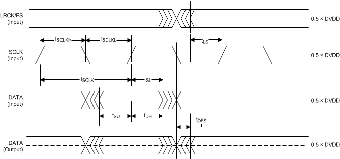 Figure 19. MCLK Timing Diagram in Slave Mode
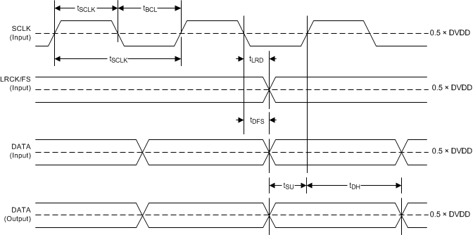 Figure 20. MCLK Timing Diagram in Master Mode
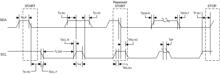 Figure 21. I2C Communication Port Timing Diagram
 Figure 22. SPK_MUTE Timing Diagram for Soft Mute Operation via Hardware Pin
7.12 Power Dissipation
| VPVDD
(V) |
SPK_GAIN(1)(2)(3)
(dBV) |
fSPK_AMP
(kHz) |
STATE OF OPERATION |
RSPK
(Ω) |
IPVDD(4)
(mA) |
IDVDD(5)
(mA) |
PDISS
(W) |
|---|---|---|---|---|---|---|---|
| 7.4 | 20 | 384 | Idle | 4 | 21.3 | 35 | 0.273 |
| 6 | 21.33 | 35 | 0.273 | ||||
| 8 | 21.3 | 35 | 0.273 | ||||
| Mute | 4 | 21.33 | 35 | 0.273 | |||
| 6 | 21.34 | 35 | 0.273 | ||||
| 8 | 21.36 | 35 | 0.274 | ||||
| Standby | 4 | 2.08 | 17 | 0.071 | |||
| 6 | 2.11 | 17 | 0.072 | ||||
| 8 | 2.17 | 17 | 0.072 | ||||
| Powerdown | 4 | 2.03 | 1 | 0.018 | |||
| 6 | 2.04 | 1 | 0.018 | ||||
| 8 | 2.06 | 1 | 0.019 | ||||
| 768 | Idle | 4 | 27.48 | 35 | 0.319 | ||
| 6 | 27.49 | 35 | 0.319 | ||||
| 8 | 24.46 | 35 | 0.297 | ||||
| Mute | 4 | 27.5 | 35 | 0.319 | |||
| 6 | 27.51 | 35 | 0.319 | ||||
| 8 | 27.52 | 35 | 0.319 | ||||
| Standby | 4 | 2.04 | 17 | 0.071 | |||
| 6 | 2.08 | 17 | 0.071 | ||||
| 8 | 2.11 | 17 | 0.072 | ||||
| Powerdown | 4 | 2.06 | 1 | 0.019 | |||
| 6 | 2.07 | 1 | 0.019 | ||||
| 8 | 2.08 | 1 | 0.019 | ||||
| 11.1 | 20 | 384 | Idle | 4 | 24.33 | 35 | 0.386 |
| 6 | 24.32 | 35 | 0.385 | ||||
| 8 | 24.36 | 35 | 0.386 | ||||
| Mute | 4 | 24.36 | 35 | 0.386 | |||
| 6 | 24.32 | 35 | 0.385 | ||||
| 8 | 24.37 | 35 | 0.386 | ||||
| Standby | 4 | 3.58 | 17 | 0.096 | |||
| 6 | 3.57 | 17 | 0.096 | ||||
| 8 | 3.58 | 17 | 0.096 | ||||
| Powerdown | 4 | 3.52 | 1 | 0.042 | |||
| 6 | 3.52 | 1 | 0.042 | ||||
| 8 | 3.54 | 1 | 0.043 | ||||
| 768 | Idle | 4 | 30.7 | 35 | 0.456 | ||
| 6 | 30.65 | 35 | 0.456 | ||||
| 8 | 30.67 | 35 | 0.456 | ||||
| Mute | 4 | 3.072 | 35 | 0.150 | |||
| 6 | 30.69 | 35 | 0.456 | ||||
| 8 | 30.69 | 35 | 0.456 | ||||
| Standby | 4 | 3.54 | 17 | 0.095 | |||
| 6 | 3.54 | 17 | 0.095 | ||||
| 8 | 3.58 | 17 | 0.096 | ||||
| Powerdown | 4 | 3.53 | 1 | 0.042 | |||
| 6 | 3.53 | 1 | 0.042 | ||||
| 8 | 3.55 | 1 | 0.043 | ||||
| 12 | 20 | 384 | Idle | 4 | 25.07 | 35 | 0.416 |
| 6 | 25.08 | 35 | 0.416 | ||||
| 8 | 25.1 | 35 | 0.417 | ||||
| Mute | 4 | 25.12 | 35 | 0.417 | |||
| 6 | 25.08 | 35 | 0.416 | ||||
| 8 | 25.11 | 35 | 0.417 | ||||
| Standby | 4 | 3.92 | 17 | 0.103 | |||
| 6 | 3.93 | 17 | 0.103 | ||||
| 8 | 3.94 | 17 | 0.103 | ||||
| Powerdown | 4 | 3.87 | 1 | 0.050 | |||
| 6 | 3.85 | 1 | 0.050 | ||||
| 8 | 3.87 | 1 | 0.050 | ||||
| 768 | Idle | 4 | 31.31 | 35 | 0.491 | ||
| 6 | 31.29 | 35 | 0.491 | ||||
| 8 | 31.31 | 35 | 0.491 | ||||
| Mute | 4 | 31.31 | 35 | 0.491 | |||
| 6 | 31.33 | 35 | 0.491 | ||||
| 8 | 31.32 | 35 | 0.491 | ||||
| Standby | 4 | 3.88 | 17 | 0.103 | |||
| 6 | 3.9 | 17 | 0.103 | ||||
| 8 | 3.91 | 17 | 0.103 | ||||
| Powerdown | 4 | 3.89 | 1 | 0.050 | |||
| 6 | 3.91 | 1 | 0.050 | ||||
| 8 | 3.88 | 1 | 0.050 | ||||
| 15 | 26 | 384 | Idle | 4 | 27.94 | 35 | 0.535 |
| 6 | 27.91 | 35 | 0.534 | ||||
| 8 | 27.75 | 35 | 0.532 | ||||
| Mute | 4 | 27.98 | 35 | 0.535 | |||
| 6 | 27.94 | 35 | 0.535 | ||||
| 8 | 27.88 | 35 | 0.534 | ||||
| Standby | 4 | 5.09 | 17 | 0.132 | |||
| 6 | 5.12 | 17 | 0.133 | ||||
| 8 | 5.19 | 17 | 0.134 | ||||
| Powerdown | 4 | 5.02 | 1 | 0.079 | |||
| 6 | 5.06 | 1 | 0.079 | ||||
| 8 | 5.14 | 1 | 0.080 | ||||
| 768 | Idle | 4 | 33.05 | 35 | 0.611 | ||
| 6 | 33.03 | 35 | 0.611 | ||||
| 8 | 33.08 | 35 | 0.612 | ||||
| Mute | 4 | 33.03 | 35 | 0.611 | |||
| 6 | 33.04 | 35 | 0.611 | ||||
| 8 | 33.05 | 35 | 0.611 | ||||
| Standby | 4 | 5.07 | 17 | 0.132 | |||
| 6 | 5.09 | 17 | 0.132 | ||||
| 8 | 5.14 | 17 | 0.133 | ||||
| Powerdown | 4 | 5.02 | 1 | 0.079 | |||
| 6 | 5.04 | 1 | 0.079 | ||||
| 8 | 5.09 | 1 | 0.080 | ||||
| 19.6 | 26 | 384 | Idle | 4 | 32.27 | 35 | 0.748 |
| 6 | 32.19 | 35 | 0.746 | ||||
| 8 | 32.08 | 35 | 0.744 | ||||
| Mute | 4 | 32.27 | 35 | 0.748 | |||
| 6 | 32.24 | 35 | 0.747 | ||||
| 8 | 32.22 | 35 | 0.747 | ||||
| Standby | 4 | 6.95 | 17 | 0.192 | |||
| 6 | 6.93 | 17 | 0.192 | ||||
| 8 | 7 | 17 | 0.193 | ||||
| Powerdown | 4 | 6.89 | 1 | 0.138 | |||
| 6 | 6.9 | 1 | 0.139 | ||||
| 8 | 6.96 | 1 | 0.140 | ||||
| 768 | Idle | 4 | 34.99 | 35 | 0.801 | ||
| 6 | 34.95 | 35 | 0.801 | ||||
| 8 | 34.97 | 35 | 0.801 | ||||
| Mute | 4 | 34.96 | 35 | 0.801 | |||
| 6 | 34.98 | 35 | 0.801 | ||||
| 8 | 34.96 | 35 | 0.801 | ||||
| Standby | 4 | 6.93 | 17 | 0.192 | |||
| 6 | 6.93 | 17 | 0.192 | ||||
| 8 | 6.98 | 17 | 0.193 | ||||
| Powerdown | 4 | 6.84 | 1 | 0.137 | |||
| 6 | 6.89 | 1 | 0.138 | ||||
| 8 | 6.9 | 1 | 0.139 | ||||
| 24 | 26 | 384 | Idle | 4 | 36.93 | 35 | 1.002 |
| 6 | 36.87 | 35 | 1.000 | ||||
| 8 | 36.77 | 35 | 0.998 | ||||
| Mute | 4 | 36.94 | 35 | 1.002 | |||
| 6 | 36.89 | 35 | 1.001 | ||||
| 8 | 36.85 | 35 | 1.000 | ||||
| Standby | 4 | 8.73 | 17 | 0.266 | |||
| 6 | 8.72 | 17 | 0.265 | ||||
| 8 | 8.71 | 17 | 0.265 | ||||
| Powerdown | 4 | 8.64 | 1 | 0.211 | |||
| 6 | 8.66 | 1 | 0.211 | ||||
| 8 | 8.69 | 1 | 0.212 | ||||
| 768 | Idle | 4 | 36.84 | 35 | 1.000 | ||
| 6 | 36.86 | 35 | 1.000 | ||||
| 8 | 36.83 | 35 | 0.999 | ||||
| Mute | 4 | 36.85 | 35 | 1.000 | |||
| 6 | 36.84 | 35 | 1.000 | ||||
| 8 | 36.82 | 35 | 0.999 | ||||
| Standby | 4 | 8.66 | 17 | 0.264 | |||
| 6 | 8.68 | 17 | 0.264 | ||||
| 8 | 8.71 | 17 | 0.265 | ||||
| Powerdown | 4 | 8.63 | 1 | 0.210 | |||
| 6 | 8.64 | 1 | 0.211 | ||||
| 8 | 8.65 | 1 | 0.211 |
7.13 Typical Characteristics
All performance plots were taken using the TAS5754M-56MEVM at room temperature, unless otherwise noted. The term Traditional LC filter refers to the output filter that is present by default on the EVM. For Filterless measurements, the on-board LC filter was removed and an Audio Precision AUX-025 measurement filter was used to take the measurements.
Table 1. Quick Reference Table
| OUTPUT CONFIGURATIONS |
PLOT TITLE | FIGURE NUMBER |
|---|---|---|
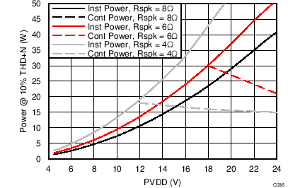
| Bridge Tied Load (BTL) Configuration Curves | Output Power vs PVDD | Figure 23 |
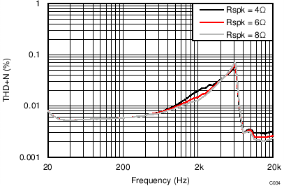
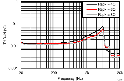
| THD+N vs Frequency, VPVDD = 12 V | Figure 24 | |
| THD+N vs Frequency, VPVDD = 15 V | Figure 25 | |
| THD+N vs Frequency, VPVDD = 18 V | Figure 26 | |
| THD+N vs Frequency, VPVDD = 24 V | Figure 27 | |
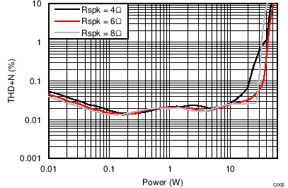
| THD+N vs Power, VPVDD = 12 V | Figure 28 | |
| THD+N vs Power, VPVDD = 15 V | Figure 29 | |
| THD+N vs Power, VPVDD = 18 V | Figure 30 | |
| THD+N vs Power, VPVDD = 24 V | Figure 31 | |
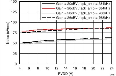
| Idle Channel Noise vs PVDD | Figure 32 | |
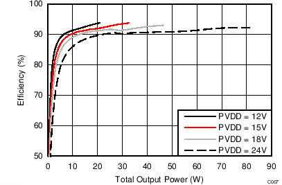
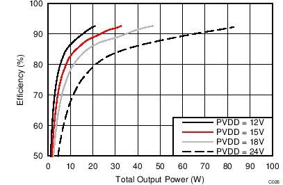
| Efficiency vs Output Power | Figure 33 | |
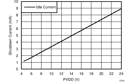
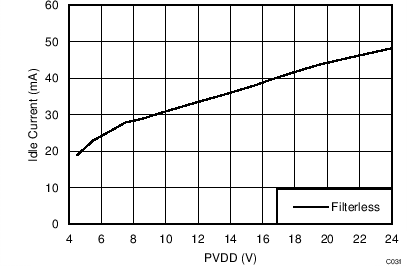
| Idle Current Draw (Filterless) vs PVDD | Figure 34 | |
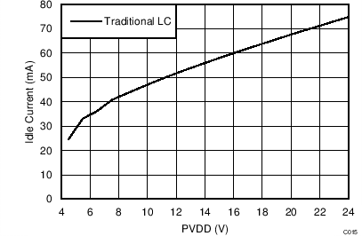
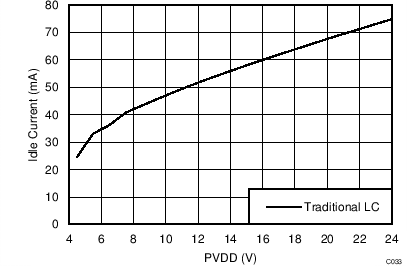
| Idle Current Draw (Traditional LC Filter) vs PVDD | Figure 35 | |
| Crosstalk vs. Frequency | Figure 36 | |
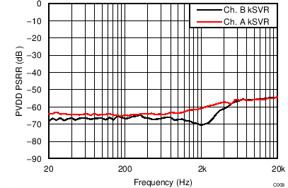
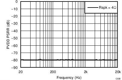
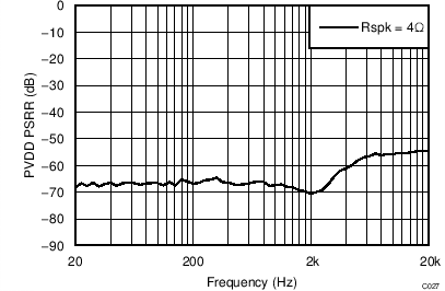
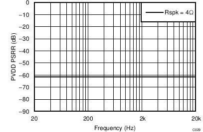
| PVDD PSRR vs Frequency | Figure 37 | |
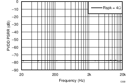
| DVDD PSRR vs Frequency | Figure 38 | |
| AVDD PSRR vs Frequency | Figure 39 | |
| CPVDD PSRR vs Frequency | Figure 40 | |
| Powerdown Current Draw vs PVDD | Figure 41 | |
| Parallel Bridge Tied Load (PBTL) Configuration | Output Power vs PVDD | Figure 42 |
| THD+N vs Frequency, VPVDD = 12 V | Figure 43 | |
| THD+N vs Frequency, VPVDD = 15 V | Figure 44 | |
| THD+N vs Frequency, VPVDD = 18 V | Figure 45 | |
| THD+N vs Frequency, VPVDD = 24 V | Figure 46 | |
| THD+N vs Power, VPVDD = 12 V | Figure 47 | |
| THD+N vs Power, VPVDD = 15 V | Figure 48 | |
| THD+N vs Power, VPVDD = 18 V | Figure 49 | |
| THD+N vs Power, VPVDD = 24 V | Figure 50 | |
| Idle Channel Noise vs PVDD | Figure 51 | |
| Efficiency vs Output Power | Figure 52 | |
| Idle Current Draw (filterless) vs PVDD | Figure 57 | |
| Idle Current Draw (traditional LC filter) vs PVDD | Figure 58 | |
| PVDD PSRR vs Frequency | Figure 53 | |
| DVDD PSRR vs Frequency | Figure 54 | |
| AVDD PSRR vs Frequency | Figure 55 | |
| CPVDD PSRR vs Frequency | Figure 56 | |
| Powerdown Current Draw vs PVDD | Figure 59 |
7.13.1 Bridge Tied Load (BTL) Configuration Curves
Return to Quick Reference Table.

| AV(SPK_AMP) = 26 dBV |
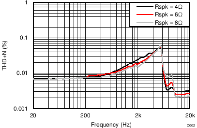
| AV(SPK_AMP) = 20 dBV | PO = 1 W | VPVDD = 15 V |
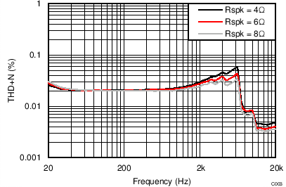
| AV(SPK_AMP)
= 26 dBV |
PO = 1 W | VPVDD = 24 V |
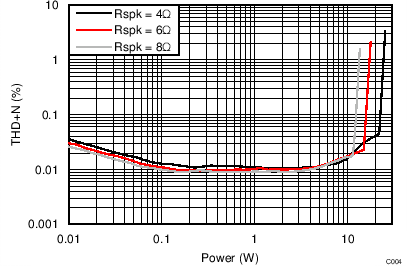
| AV(SPK_AMP)
= 20 dBV |
Input Signal = 1 kHz Sine | VPVDD = 15 V |
| AV(SPK_AMP) = 26 dBV | PO = 1 W | VPVDD = 24 V |
| RSPK = 8 Ω |
| fSPK_AMP = 768 kHz | RSPK = 8 Ω |
(Traditional LC Filter) vs PVDD – BTL
| AV(SPK_AMP) = 26 dBV | Supply Noise = 250 mV |
| VPVDD = 24 V | Sine Input |
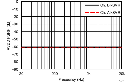
| AV(SPK_AMP) = 26 dBV | Supply Noise = 250 mV |
| VPVDD = 24 V | RSPK = 8 Ω |
| AV(SPK_AMP) = 26 dBV | fSPK_AMP = 786 kHz | |
| AV(SPK_AMP) = 20 dBV | PO = 1 W | VPVDD = 12 V |
| AV(SPK_AMP) = 20 dBV | PO = 1 W | VPVDD = 18 V |
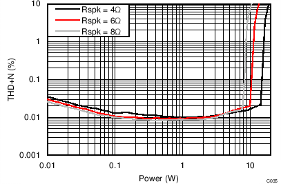
| AV(SPK_AMP)
= 20 dBV |
Input Signal = 1 kHz Sine | VPVDD = 12 V |
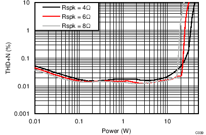
| AV(SPK_AMP)
= 26 dBV |
Input Signal = 1 kHz Sine | VPVDD = 18 V |
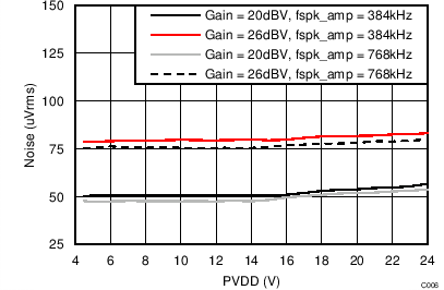
| AV(SPK_AMP) = 20 dBV | fSPK_AMP = 384 kHz | RSPK = 8 Ω |
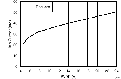
| fSPK_AMP = 768 kHz | RSPK = 8 Ω |
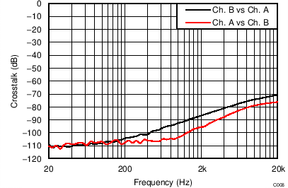
| AV(SPK_AMP) = 26 dBV | Sine Input | VPVDD = 24 V |
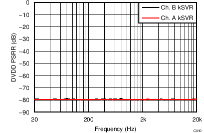
| AV(SPK_AMP) = 26 dBV | Supply Noise = 250 mV |
| VPVDD = 24 V | RSPK = 8 Ω |
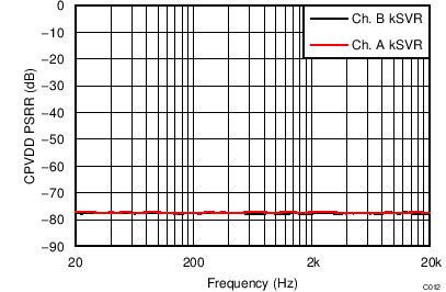
| AV(SPK_AMP) = 26 dBV | Supply Noise = 250 mV |
| VPVDD = 24 V | Sine Input |
7.13.2 Parallel Bridge Tied Load (PBTL) Configuration
Return to Quick Reference Table.
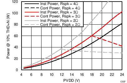
| AV(SPK_AMP) = 26 dBV | Measured on TAS5754/6 EVM | |
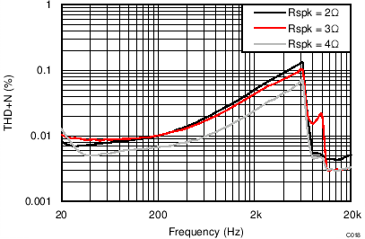
| AV(SPK_AMP) = 20 dBV | PO = 1 W | VPVDD = 15 V |
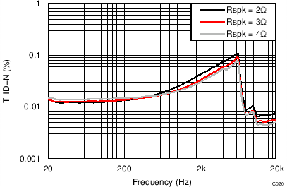
| AV(SPK_AMP) = 26 dBV | PO = 1 W | VPVDD = 24 V |
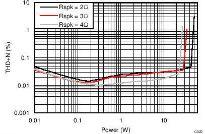
| AV(SPK_AMP) = 20 dBV |
PO = 1 W | VPVDD = 15 V |
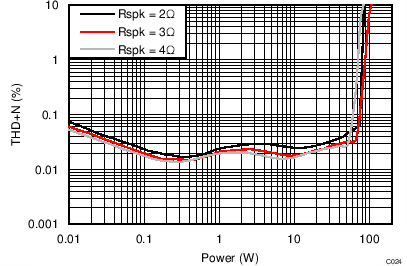
| AV(SPK_AMP) = 20 dBV | PO = 1 W |
| VPVDD = 24 V | Input Signal = 1 kHz Sine |
| AV(SPK_AMP) = 26 dBV | ILOAD = xA | VPVDD = 24 V |
| AV(SPK_AMP) = 26 dBV | RSPK = 8 Ω |
| VPVDD = 24 V | Supply Noise = 250 mV |
| AV(SPK_AMP) = 26 dBV | Sine Input |
| VPVDD = 24 V | Supply Noise = 250 mV |
(Traditional LC filter) vs PVDD – PBTL
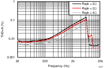
| AV(SPK_AMP) = 20 dBV | PO = 1 W | VPVDD = 12 V |
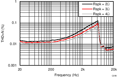
| AV(SPK_AMP) = 26 dBV | PO = 1 W | VPVDD = 18 V |
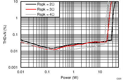
| AV(SPK_AMP) = 20 dBV | PO = 1 W | VPVDD = 12 V |
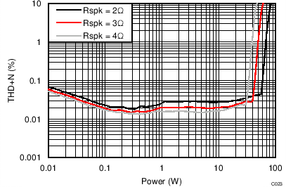
| AV(SPK_AMP) = 20 dBV | PO = 1 W |
| VPVDD = 18 V | Input Signal = 1 kHz Sine |
| AV(SPK_AMP)
= 26 dBV |
ILOAD = xA | VPVDD = 18 V |
| AV(SPK_AMP) = 26dBV | Sine Input | VPVDD = 24V |
| AV(SPK_AMP) = 26 dBV | RSPK = 8 Ω |
| VPVDD = 24 V | Supply Noise = 250 mV |
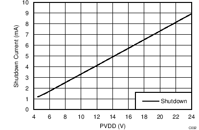
| AV(SPK_AMP) = 26 dBV | fSPK_AMP = 786 kHz |