-
TPS6206x-Q1 Functional Safety FIT Rate, FMD and Pin FMA SLVAEO9B February 2020 – January 2021 TPS62065-Q1 , TPS62067-Q1
-
TPS6206x-Q1 Functional Safety FIT Rate, FMD and Pin FMA
TPS6206x-Q1 Functional Safety FIT Rate, FMD and Pin FMA
1 Overview
This document contains information for TPS6206x-Q1 (WSON package) to aid in a functional safety system design. Information provided are:
- Functional Safety Failure In Time (FIT) rates of the semiconductor component estimated by the application of industry reliability standards
- Component failure modes and their distribution (FMD) based on the primary function of the device
- Pin failure mode analysis (Pin FMA)
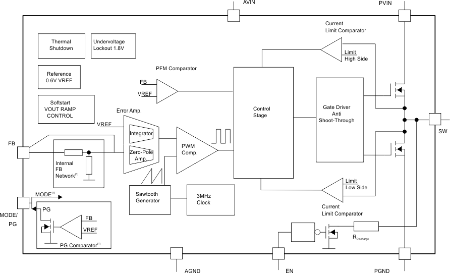
Figure 1-1 shows the device functional block diagram for reference.
 Figure 1-1 Functional Block Diagram
TPS6206x-Q1 was developed using a quality-managed development process, but was not developed in accordance with the IEC 61508 or ISO 26262 standards.
2 Functional Safety Failure In Time (FIT) Rates
This section provides Functional Safety Failure In Time (FIT) rates for TPS6206x-Q1 based on an industry-wide used reliability standard:
- Table 2-1 provides FIT rates based on IEC TR 62380 / ISO 26262 part 11.
- Table 2-2 provides FIT rates based on the Siemens Norm SN 29500-2
| FIT IEC TR 62380 / ISO 26262 | FIT (Failures Per 109 Hours) |
|---|---|
| Total Component FIT Rate | 5 |
| Die FIT Rate | 3 |
| Package FIT Rate | 2 |
The failure rate and mission profile information in Table 2-1 comes from the Reliability data handbook IEC TR 62380 / ISO 26262 part 11:
- Mission profile: motor control
- Power dissipation: 300 mW
- Climate type: world-wide Table 8
- Package factor (lambda 3): Table 17b
- Substrate Material: FR4
- EOS FIT rate assumed: 0 FIT
| Table | Category | Reference FIT Rate | Reference Virtual TJ |
|---|---|---|---|
| 5 | CMOS,
BICMOS Digital, analog / mixed |
25 FIT | 55°C |
The Reference FIT Rate and Reference Virtual TJ (junction temperature) in Table 2-2 come from the Siemens Norm SN 29500-2 tables 1 through 5. Failure rates under operating conditions are calculated from the reference failure rate and virtual junction temperature using conversion information in SN 29500-2 section 4.
3 Failure Mode Distribution (FMD)
The failure mode distribution estimation for TPS6206x-Q1 in Table 3-1 comes from the combination of common failure modes listed in standards such as IEC 61508 and ISO 26262, the ratio of sub-circuit function size and complexity and from best engineering judgment.
The failure modes listed in this section reflect random failure events and do not include failures due to misuse or overstress.
| Die Failure Modes | Failure Mode Distribution (%) |
|---|---|
| SW no output | 35% |
| SW output not in specification - voltage or timing | 45% |
| SW power HS or LS FET stuck on | 15% |
| Short circuit any two pins | 5% |
4 Pin Failure Mode Analysis (Pin FMA)
This section provides a Failure Mode Analysis (FMA) for the pins of the TPS6206x-Q1. The failure modes covered in this document include the typical pin-by-pin failure scenarios:
- Pin short-circuited to PGND or AGND (see Table 4-2)
- Pin open-circuited (see Table 4-3)
- Pin short-circuited to an adjacent pin (see Table 4-4)
- Pin short-circuited to AVIN or PVIN (see Table 4-5)
Table 4-2 through Table 4-5 also indicate how these pin conditions can affect the device as per the failure effects classification in Table 4-1.
| Class | Failure Effects |
|---|---|
| A | Potential device damage that affects functionality |
| B | No device damage, but loss of functionality |
| C | No device damage, but performance degradation |
| D | No device damage, no impact to functionality or performance |
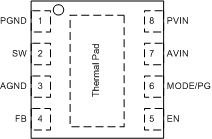
Figure 4-1 shows the TPS6206x-Q1 pin diagram. For a detailed description of the device pins please refer to the 'Pin Configuration and Functions' section in the TPS6206x-Q1 data sheet.
 Figure 4-1 Pin Diagram
Following are the assumptions of use and the device configuration assumed for the pin FMA in this section:
- Assumption the device is running in the typical application. Please refer to the 'Typical Application Circuit' on the 1st page in the TPS6206x-Q1 datasheet.
| Pin Name | Pin No. | Description of Potential Failure Effect(s) | Failure Effect Class |
|---|---|---|---|
| PGND | 1 | Intended connection | D |
| SW | 2 | Potential internal device damage | A |
| AGND | 3 | Intended connection | D |
| FB | 4 | Device not functional: Missing feedback path (Open Loop operation); output voltage out of spec; potential device damage | A |
| EN | 5 | Intended connection: Device disabled | D |
| MODE | 6 | TPS62065-Q1: Intended connection: Enabling power safe mode with automatic transition from PFM to fixed frequency PWM mode | D |
| PG | 6 | TPS62067-Q1: Intended connection in case PG not used | D |
| AVIN | 7 | Device not functional; supply short to ground | B |
| PVIN | 8 | Device not functional; supply short to ground | B |
| Pin Name | Pin No. | Description of Potential Failure Effect(s) | Failure Effect Class |
|---|---|---|---|
| PGND | 1 | Internal ground shift; device not functional; potential internal damage | A |
| SW | 2 | Device not function - open loop operation | B |
| AGND | 3 | Internal ground shift; device not functional; potential internal damage | A |
| FB | 4 | Device not functional - open loop operation | B |
| EN | 5 | Undetermined state of pin EN; spec violation; potentially increased quiescent current | C |
| MODE | 6 | TPS62065-Q1: Undetermined state of pin MODE/PG spec violation; potentially increased quiescent current | C |
| PG | 6 | TPS62067-Q1: Intended connection in case PG not used | D |
| AVIN | 7 | Missing power supply - device not functional | B |
| PVIN | 8 | Missing power supply - device not functional | B |
| Pin Name | Pin No. | Shorted to | Description of Potential Failure Effect(s) | Failure Effect Class |
|---|---|---|---|---|
| PGND | 1 | SW | Potential internal device damage | A |
| SW | 2 | AGND | Potential internal device damage | A |
| AGND | 3 | FB | Device not functional: Missing feedback path (Open Loop operation); output voltage out of spec; potential device damage | A |
| EN | 5 | MODE | TPS62065-Q1: Intended connection: Device operation in fixed frequency PWM mode | D |
| EN | 5 | PG | TPS62067-Q1: Potential internal damage | A |
| MODE | 6 | AVIN | TPS62065-Q1: Intended connection: Device operation in fixed frequency PWM mode | D |
| PG | 6 | AVIN | TPS62067-Q1: Potential internal damage | A |
| AVIN | 7 | PVIN | Intended connection | D |
| Pin Name | Pin No. | Description of Potential Failure Effect(s) | Failure Effect Class |
|---|---|---|---|
| PGND | 1 | Device not functional; supply short to ground | B |
| SW | 2 | Potential internal device damage | A |
| AGND | 3 | Device not functional; supply short to ground | B |
| FB | 4 | Device not functional: Missing feedback path (Open Loop operation); output voltage out of spec; potential device damage | A |
| EN | 5 | Intended connection: Device enabled | D |
| MODE | 6 | TPS62065-Q1: Intended connection: Device operation in fixed frequency PWM mode | D |
| PG | 6 | TPS62067-Q1: Potential internal damage | A |
| AVIN | 7 | Intended connection | D |
| PVIN | 8 | Intended connection | D |