TPS54160 1.5-A, 60-V, Step-Down DC/DC Converter with Eco-mode™
1 Features
- 3.5 V to 60 V Input Voltage Range
- 200-mΩ High-Side MOSFET
- High Efficiency at Light Loads with a Pulse Skipping Eco-mode™
- TPS54160A has Tighter Enable Threshold Than TPS54160 for More Accurate UVLO voltage
- Adjustable UVLO Voltage and Hysteresis
- 116 μA Operating Quiescent Current
- 1.3 μA Shutdown Current
- 100 kHz to 2.5 MHz Switching Frequency
- Synchronizes to External Clock
- Adjustable Slow Start/Sequencing
- UV and OV Power Good Output
- 0.8-V Internal Voltage Reference
- MSOP10 and 3mm x 3mm VSON Package with PowerPAD™
- Supported by WEBBENCH® and SwitcherPro™ Software Tool
2 Applications
- 12-V, 24-V and 48-V Industrial and Commercial Low Power Systems
- Aftermarket Auto Accessories: Video, GPS, Entertainment
3 Description
The TPS54160A device is a 60-V, 1.5-A, step down regulator with an integrated high-side MOSFET. Current mode control provides simple external compensation and flexible component selection. A low ripple pulse skip mode reduces the no load, regulated output supply current to 116 μA. Using the enable pin, shutdown supply current is reduced to 1.3 μA.
Under voltage lockout is internally set at 2.5 V, but can be increased using the enable pin. The output voltage startup ramp is controlled by the slow start pin that can also be configured for sequencing/tracking. An open drain power good signal indicates the output is within 94% to 107% of its nominal voltage.
A wide switching frequency range allows efficiency and external component size to be optimized. Frequency fold back and thermal shutdown protects the part during an overload condition.
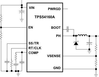
4 Simplified Schematic
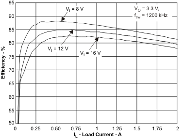
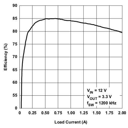
4.0.1 Efficiency vs Load Current
5 Revision History
Changes from B Revision (January 2014) to C Revision
- Deleted SWIFT from the data sheet Title and FeaturesGo
- Changed Feature From: Tighter Enable Threshold Than TPS54160 ... To: TPS54160A has Tighter Enable Threshold Than TPS54160 for More Accurate UVLO voltageGo
- Added the Device Information tableGo
- Deleted the Ordering Information table Go
- Added the Handling Ratings tableGo
- Added the Recommended Operating Conditions tableGo
- Changed the Enable threshold voltage to include values for TPS54160 and TPS54160A Go
- Added the Power Supply Recommendations sectionGo
Changes from A Revision (July 2012) to B Revision
- Deleted SWIFT from the data sheet Title and FeaturesGo
- Changed text in the Description From: "within 93% to 107% of its nominal voltage." To: "within 94% to 107% of its nominal voltage."Go
- Changed the values of the Hysteresis current in the Electrical Characteristics tableGo
- Changed text in the Error Amplifier section From: "the transconductance is 25 μA/V" To: "the transconductance is 26 μA/V" Go
- Changed text in the Slow Start and Tracking Pin (SS/TR) section From: "VIN UVLO is excedded, EN pin pulled below 1.25V" To: "VIN pin is below the VIN UVLO, EN pin pulled below 1.25V"Go
- Changed Start Input Voltage (rising VIN) voltage From: 7.25 V To: 7.7 VGo
- Changed Start Input Voltage (falling VIN) voltage From: 6.25 V To: 6.7 VGo
- Changed Equation 29Go
- Changed Equation 32Go
- Changed 7.25V to 7.7V and 6.25V to 6.7V in the Under Voltage Lock Out Set Point section.Go
- Changed Equation 41 and Equation 42Go
- Changed Equation 47Go
- Changed Equation 49, Equation 52, and Equation 53Go
Changes from * Revision (May 2012) to A Revision
- Changed text in the Description From: "within 93% to 107% of its nominal voltage." To: "within 94% to 107% of its nominal voltage."Go
- Changed the values of the Hysteresis current in the Electrical Characteristics tableGo
- Changed text in the Error Amplifier section From: "the transconductance is 25 μA/V" To: "the transconductance is 26 μA/V" Go
- Changed text in the Slow Start and Tracking Pin (SS/TR) section From: "VIN UVLO is excedded, EN pin pulled below 1.25V" To: "VIN pin is below the VIN UVLO, EN pin pulled below 1.25V"Go
- Changed Start Input Voltage (rising VIN) voltage From: 7.25 V To: 7.7 VGo
- Changed Start Input Voltage (falling VIN) voltage From: 6.25 V To: 6.7 VGo
- Changed Equation 29Go
- Changed Equation 32Go
- Changed 7.25V to 7.7V and 6.25V to 6.7V in the Under Voltage Lock Out Set Point section.Go
- Changed Equation 41 and Equation 42Go
- Changed Equation 47Go
- Changed Equation 49, Equation 52, and Equation 53Go
6 Terminal Configuration and Functions

Terminal Functions
| TERMINAL | I/O | DESCRIPTION | ||
|---|---|---|---|---|
| NAME | NO. | |||
| BOOT | 1 | O | A bootstrap capacitor is required between BOOT and PH. If the voltage on this capacitor is below the minimum required by the device, the output is forced to switch off until the capacitor is refreshed. | |
| COMP | 8 | O | Error amplifier output, and input to the output switch current comparator. Connect frequency compensation components to this pin. | |
| EN | 3 | I | Enable pin, internal pull-up current source. Pull below 1.2 V to disable. Float to enable. Adjust the input undervoltage lockout with two resistors. | |
| GND | 9 | – | Ground | |
| PH | 10 | O | The source of the internal high-side power MOSFET. | |
| Thermal Pad | 11 | – | GND pin must be electrically connected to the exposed pad on the printed circuit board for proper operation. | |
| PWRGD | 6 | O | An open drain output, asserts low if output voltage is low due to thermal shutdown, dropout, over-voltage or EN shut down. | |
| RT/CLK | 5 | I | Resistor Timing and External Clock. An internal amplifier holds this pin at a fixed voltage when using an external resistor to ground to set the switching frequency. If the pin is pulled above the PLL upper threshold, a mode change occurs and the pin becomes a synchronization input. The internal amplifier is disabled and the pin is a high impedance clock input to the internal PLL. If clocking edges stop, the internal amplifier is re-enabled and the mode returns to a resistor set function. | |
| SS/TR | 4 | I/O | Slow-start and Tracking. An external capacitor connected to this pin sets the output rise time. Since the voltage on this pin overrides the internal reference, it can be used for tracking and sequencing. | |
| VIN | 2 | I | Input supply voltage, 3.5 V to 60 V. | |
| VSENSE | 7 | I | Inverting node of the transconductance (gM) error amplifier. | |
7 Specifications
7.1 Absolute Maximum Ratings(1)
Over operating temperature range (unless otherwise noted).| VALUE | UNIT | |||
|---|---|---|---|---|
| MIN | MAX | |||
| Input voltage | VIN | –0.3 | 65 | V |
| EN(2) | –0.3 | 5 | ||
| BOOT | 73 | |||
| VSENSE | –0.3 | 3 | ||
| COMP | –0.3 | 3 | ||
| PWRGD | –0.3 | 6 | ||
| SS/TR | –0.3 | 3 | ||
| RT/CLK | –0.3 | 3.6 | ||
| Output voltage | BOOT-PH | 8 | V | |
| PH | –0.6 | 65 | ||
| PH, 10-ns Transient | –2 | 65 | ||
| Voltage Difference | PAD to GND | ±200 | mV | |
| Source current | EN | 100 | μA | |
| BOOT | 100 | mA | ||
| VSENSE | 10 | μA | ||
| PH | Current Limit | A | ||
| RT/CLK | 100 | μA | ||
| Sink current | VIN | Current Limit | A | |
| COMP | 100 | μA | ||
| PWRGD | 10 | mA | ||
| SS/TR | 200 | μA | ||
| Operating junction temperature | –40 | 150 | °C | |
7.2 Handling Ratings
| MIN | MAX | UNIT | |||
|---|---|---|---|---|---|
| TSTG | Storage temperature | –65 | 150 | °C | |
| VESD(1) | Human Body Model (HBM) ESD Stress Voltage (2) QSS 009-105 (JESD22-A114A) |
TPS54160 | 1 | kV | |
| Human Body Model (HBM) ESD Stress Voltage (2) QSS 009-105 (JESD22-A114A) |
TPS54160A | 2 | kV | ||
| Charged Device Model (CDM) ESD Stress Voltage (3) QSS 009-147 (JESD22-C101B.01) |
500 | V | |||
7.3 Recommended Operating Conditions
over operating free-air temperature range (unless otherwise noted)| MIN | MAX | UNIT | ||
|---|---|---|---|---|
| VIN | Supply input voltage range | 3.5 | 60 | V |
| VO | Output voltage range | 0.8 | 58 | V |
| IO | Output current range | 0 | 1.5 | A |
| TJ | Junction Temperature | –40 | 150 | °C |
7.4 Thermal Information
| THERMAL METRIC(1) | TPS54160 TPS54160A |
UNITS | ||
|---|---|---|---|---|
| DGQ (10 PINS) | DRC (10 PINS) | |||
| θJA | Junction-to-ambient thermal resistance (standard board) | 62.5 | 40 | °C/W |
| θJCtop | Junction-to-case (top) thermal resistance | 83 | 65 | |
| θJB | Junction-to-board thermal resistance | 28 | 8 | |
| ψJT | Junction-to-top characterization parameter | 1.7 | 0.6 | |
| ψJB | Junction-to-board characterization parameter | 20.1 | 7.5 | |
| θJCbot | Junction-to-case (bottom) thermal resistance | 21 | 7.8 | |
7.5 Electrical Characteristics
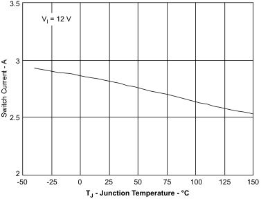
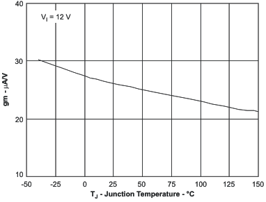
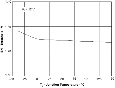
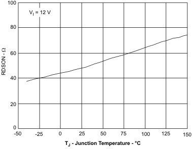
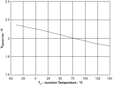
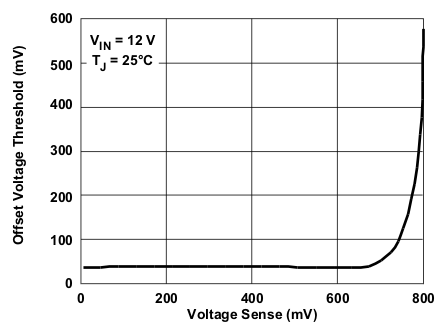
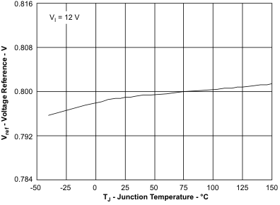
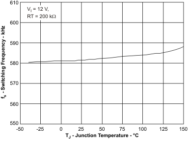
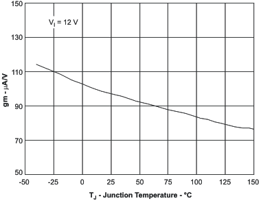
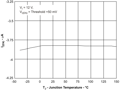
TJ = –40°C to 150°C, VIN = 3.5 to 60V (unless otherwise noted)7.6 Typical Characteristics
8 Detailed Description
8.1 Overview
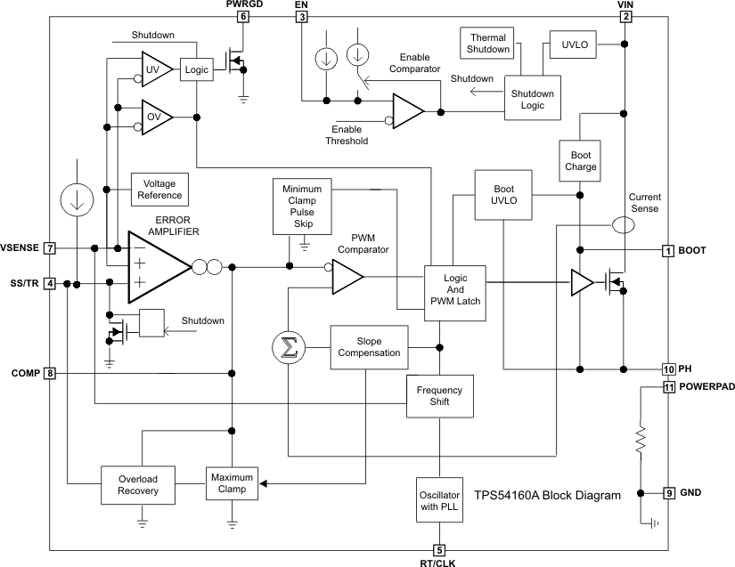
The TPS54160A device is a 60-V, 1.5-A, step-down (buck) regulator with an integrated high-side n-channel MOSFET. To improve performance during line and load transients the device implements a constant frequency, current mode control which reduces output capacitance and simplifies external frequency compensation design. The wide switching frequency of 100kHz to 2500kHz allows for efficiency and size optimization when selecting the output filter components. The switching frequency is adjusted using a resistor to ground on the RT/CLK pin. The device has an internal phase lock loop (PLL) on the RT/CLK pin that is used to synchronize the power switch turn on to a falling edge of an external system clock.
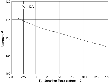
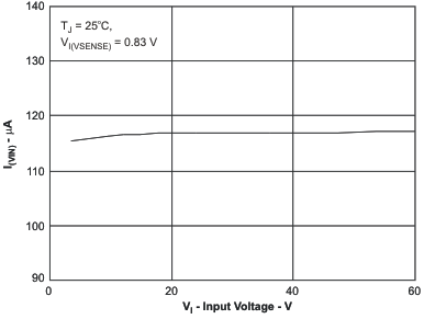
The TPS54160A has a default start up voltage of approximately 2.5V. The EN pin has an internal pull-up current source that can be used to adjust the input voltage under voltage lockout (UVLO) threshold with two external resistors. In addition, the pull up current provides a default condition. When the EN pin is floating the device operates. The operating current is 116 μA when not switching and under no load. When the device is disabled, the supply current is 1.3 μA.
The integrated 200mΩ high-side MOSFET allows for high efficiency power supply designs capable of delivering 1.5 A of continuous current to a load. The TPS54160A reduces the external component count by integrating the boot recharge diode. The bias voltage for the integrated high-side MOSFET is supplied by a capacitor on the BOOT to PH pin. The boot capacitor voltage is monitored by an UVLO circuit and turns on the high-side MOSFET off when the boot voltage falls below a preset threshold. The TPS54160A can operate at high duty cycles because of the boot UVLO. The output voltage can be stepped down to as low as the 0.8V reference.
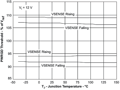
The TPS54160A has a power good comparator (PWRGD) which asserts when the regulated output voltage is less than 92% or greater than 109% of the nominal output voltage. The PWRGD pin is an open drain output which deasserts when the VSENSE pin voltage is between 94% and 107% of the nominal output voltage allowing the pin to transition high when a pull-up resistor is used.
The TPS54160A minimizes excessive output overvoltage (OV) transients by taking advantage of the OV power good comparator. When the OV comparator is activated, the high-side MOSFET is turned off and masked from turning on until the output voltage is lower than 107%.
The SS/TR (slow start/tracking) pin is used to minimize inrush currents or provide power supply sequencing during power up. A small value capacitor should be coupled to the pin to adjust the slow start time. A resistor divider can be coupled to the pin for critical power supply sequencing requirements. The SS/TR pin is discharged before the output powers up. This discharging ensures a repeatable restart after an over-temperature fault, UVLO fault or a disabled condition.
The TPS54160A, also, discharges the slow start capacitor during overload conditions with an overload recovery circuit. The overload recovery circuit will slow start the output from the fault voltage to the nominal regulation voltage once a fault condition is removed. A frequency foldback circuit reduces the switching frequency during startup and overcurrent fault conditions to help control the inductor current.
8.2 Functional Block Diagram
8.3 Feature Description
8.3.1 Fixed Frequency PWM Control
The TPS54160A uses an adjustable fixed frequency, peak current mode control. The output voltage is compared through external resistors on the VSENSE pin to an internal voltage reference by an error amplifier which drives the COMP pin. An internal oscillator initiates the turn on of the high-side power switch. The error amplifier output is compared to the high-side power switch current. When the power switch current reaches the level set by the COMP voltage, the power switch is turned off. The COMP pin voltage will increase and decrease as the output current increases and decreases. The device implements a current limit by clamping the COMP pin voltage to a maximum level. The Eco-mode™ is implemented with a minimum clamp on the COMP pin.
8.3.2 Slope Compensation Output Current
The TPS54160A adds a compensating ramp to the switch current signal. This slope compensation prevents sub-harmonic oscillations. The available peak inductor current remains constant over the full duty cycle range.
8.3.3 Pulse Skip Eco-mode
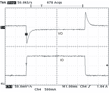
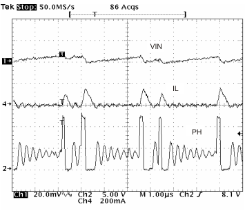
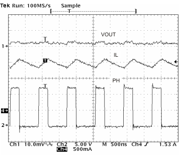
The TPS54160A enters the pulse skip mode when the voltage on the COMP pin is the minimum clamp value. The TPS54160A operates in a pulse skip mode at light load currents to improve efficiency. The peak switch current during the pulse skip mode will be the greater value of 50mA or the peak inductor current that is a function of the minimum on time, input voltage, output voltage and inductance value. When the load current is low and the output voltage is within regulation the device will enter a sleep mode and draw only 116 μA input quiescent current. While the device is in sleep mode the output power is delivered by the output capacitor. As the load current decreases, the time the output capacitor supplies the load current increases and the switching frequency decreases reducing gate drive and switching losses. As the output voltage drops, the TPS54160A wakes up from the sleep mode and the power switch turns on to recharge the output capacitor, see Figure 25. The internal PLL remains operating when in sleep mode. When operating at light load currents in the pulse skip mode the switching transitions occur synchronously with the external clock signal.
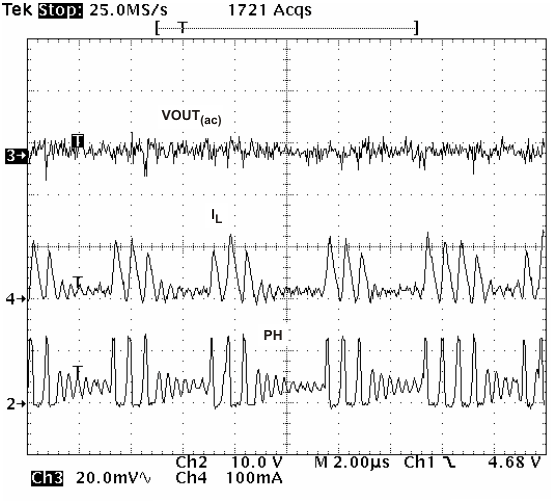 Figure 25. Pulse Skip Mode Operation
8.3.4 Bootstrap Voltage (BOOT)
The TPS54160A has an integrated boot regulator and requires a small ceramic capacitor between the BOOT and PH pin to provide the gate drive voltage for the high side MOSFET. The value of the ceramic capacitor should be 0.1 μF. A ceramic capacitor with an X7R or X5R grade dielectric is recommended because of the stable characteristics over temperature and voltage. To improve drop out, the TPS54160A is designed to operate at 100% duty cycle as long as the BOOT to PH pin voltage is greater than 2.1 V. When the voltage from BOOT to PH drops below 2.1 V, the high side MOSFET is turned off using an UVLO circuit allowing for the low side diode to conduct which allows refreshing of the BOOT capacitor. Since the supply current sourced from the BOOT capacitor is low, the high side MOSFET can remain on for more switching cycles than it refreshes, thus, the effective duty cycle limitation that is attributed to the boot regulator system is high.
8.3.5 Low Dropout Operation
The duty cycle during dropout of the regulator will be mainly determined by the voltage drops across the power MOSFET, inductor, low side diode and printed circuit board resistance. During operating conditions in which the input voltage drops, the high side MOSFET can remain on for 100% of the duty cycle to maintain output regulation or until the BOOT to PH voltage falls below 2.1 V.
Once the high side is off, the low side diode will conduct and the BOOT capacitor will be recharged. During this boot capacitor recharge time, the inductor current will ramp down until the high side MOSFET turns on. The recharge time is longer than the typical high side off time of previous switching cycles, and thus, the inductor current ripple is larger resulting in more ripple voltage on the output. The recharge time is a function of the input voltage, boot capacitor value, and the impedance of the internal boot recharge diode.
Attention needs to be taken in maximum duty cycle applications which experience extended time periods without a load current. When the voltage across the BOOT capacitors falls below the 2.1 V threshold in applications that have a difference in the input voltage and output voltage that is less than 3V, the high side MOSFET will be turned off but there is not enough current in the inductor to pull the PH pin down to recharge the boot capacitor. The regulator will not switch because the boot capacitor is less than 2.1V and the output capacitor will decay until the difference in the input voltage and output voltage is 2.1 V. At this time the boot under voltage lockout is exceeded and the device will switch until the desired output voltage is reached.
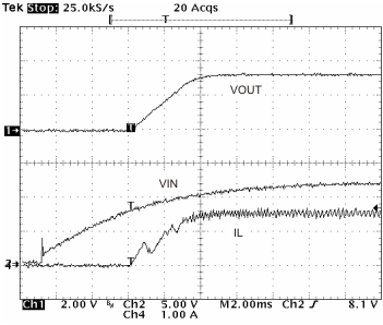
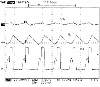
The start and stop voltages are shown in Figure 26 and Figure 27. The voltages are plotted versus load current. The start voltage is defined as the input voltage needed to regulate the output within 1%. The stop voltage is defined as the input voltage at which the output drops by 5% or stops switching.
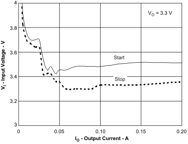 Figure 26. 3.3V Start/Stop Voltage
 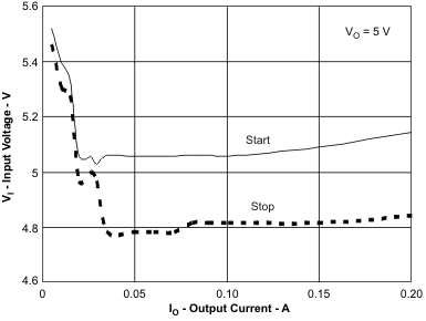 Figure 27. 5.0V Start/Stop Voltage
 8.3.6 Error Amplifier
The TPS54160A has a transconductance amplifier for the error amplifier. The error amplifier compares the VSENSE voltage to the lower of the SS/TR pin voltage or the internal 0.8-V voltage reference. The transconductance (gM) of the error amplifier is 97 μA/V during normal operation. During the slow start operation, the transconductance is a fraction of the normal operating transconductance. When the voltage of the VSENSE pin is below 0.8 V and the device is regulating using the SS/TR voltage, the transconductance is 26 μA/V.
The frequency compensation components (capacitor, series resistor and capacitor) are added to the COMP pin to ground.
8.3.7 Voltage Reference
The voltage reference system produces a precise ±2% voltage reference over temperature by scaling the output of a temperature stable bandgap circuit.
8.3.8 Adjusting the Output Voltage
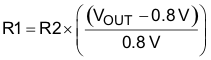
The output voltage is set with a resistor divider from the output node to the VSENSE pin. It is recommended to use 1% tolerance or better divider resistors. Start with a 10 kΩ for the R2 resistor and use the Equation 1 to calculate R1. To improve efficiency at light loads consider using larger value resistors. If the values are too high, the regulator becomes more susceptible to noise and voltage errors from the VSENSE input current are noticeable.
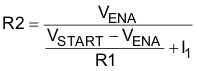
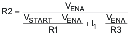
8.3.9 Enable and Adjusting Undervoltage Lockout
The TPS54160A is disabled when the VIN pin voltage falls below 2.5 V. If an application requires a higher undervoltage lockout (UVLO), use the EN pin as shown in Figure 28 to adjust the input voltage UVLO by using the two external resistors. Though it is not necessary to use the UVLO adjust registers, for operation it is highly recommended to provide consistent power up behavior. The EN pin has an internal pull-up current source, I1, of 0.9μA that provides the default condition of the TPS54160A operating when the EN pin floats. Once the EN pin voltage exceeds 1.25V, an additional 2.9 μA of hysteresis, Ihys, is added. This additional current facilitates input voltage hysteresis. Use Equation 2 to set the external hysteresis for the input voltage. Use Equation 3 to set the input start voltage.
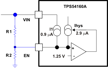 Figure 28. Adjustable Undervoltage Lockout (UVLO)
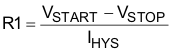
Another technique to add input voltage hysteresis is shown in Figure 29. This method may be used, if the resistance values are high from the previous method and a wider voltage hysteresis is needed. The resistor R3 sources additional hysteresis current into the EN pin.
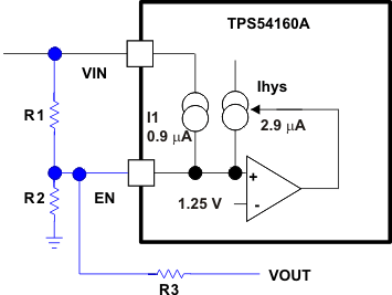 Figure 29. Adding Additional Hysteresis
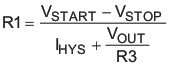
Do not place a low-impedance voltage source with greater than 5 V directly on the EN pin. Do not place a capacitor directly on the EN pin if VEN > 5 V when using a voltage divider to adjust the start and stop voltage. The node voltage, (see Figure 30) must remain equal to or less than 5.8 V. The zener diode can sink up to 100 µA. The EN pin voltage can be greater than 5 V if the VIN voltage source has a high impedance and does not source more than 100 µA into the EN pin.
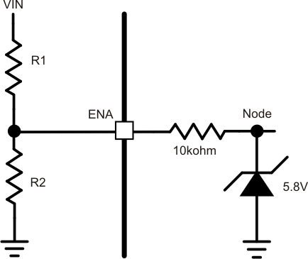 Figure 30. Node Voltage
8.3.10 Slow Start and Tracking Pin (SS/TR)
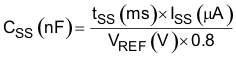
The TPS54160A effectively uses the lower voltage of the internal voltage reference or the SS/TR pin voltage as the power-supply's reference voltage and regulates the output accordingly. A capacitor on the SS/TR pin to ground implements a slow start time. The TPS54160A has an internal pull-up current source of 2μA that charges the external slow start capacitor. The calculations for the slow start time (10% to 90%) are shown in Equation 6. The voltage reference (VREF) is 0.8 V and the slow start current (ISS) is 2μA. The slow start capacitor should remain lower than 0.47 μF and greater than 0.47 nF.
At power up, the TPS54160A does not start switching until the slow start pin is discharged to less than 40 mV to ensure a proper power up, see Figure 31.
Also, during normal operation, the TPS54160A stops switching and the SS/TR must be discharged to 40 mV when the voltage at the VIN pin is below the VIN UVLO, EN pin pulled below 1.25 V, or a thermal shutdown event occurs.
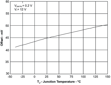
The VSENSE voltage follows the SS/TR pin voltage with a 45 mV offset up to 85% of the internal voltage reference. When the SS/TR voltage is greater than 85% on the internal reference voltage the offset increases as the effective system reference transitions from the SS/TR voltage to the internal voltage reference (see Figure 23). The SS/TR voltage ramps linearly until clamped at 1.7 V.
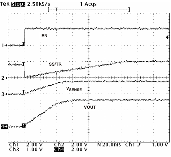 Figure 31. Operation of SS/TR Pin when Starting
8.3.11 Overload Recovery Circuit
The TPS54160A has an overload recovery (OLR) circuit. The OLR circuit slow starts the output from the overload voltage to the nominal regulation voltage once the fault condition is removed. The OLR circuit discharges the SS/TR pin to a voltage slightly greater than the VSENSE pin voltage using an internal pull down of 100 μA when the error amplifier is changed to a high voltage from a fault condition. When the fault condition is removed, the output slow-starts from the fault voltage to nominal output voltage.
8.3.12 Sequencing
Many of the common power supply sequencing methods can be implemented using the SS/TR, EN and PWRGD pins. The sequential method can be implemented using an open drain output of a power on reset pin of another device. The sequential method is illustrated in Figure 32 using two TPS54160A devices. The power good is coupled to the EN pin on the TPS54160A which enables the second power supply once the primary supply reaches regulation. If needed, a 1nF ceramic capacitor on the EN pin of the second power supply provides a 1-ms start-up delay. Figure 33 shows the results of Figure 32.
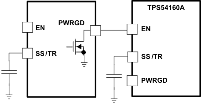 Figure 32. Schematic for Sequential Start-Up Sequence
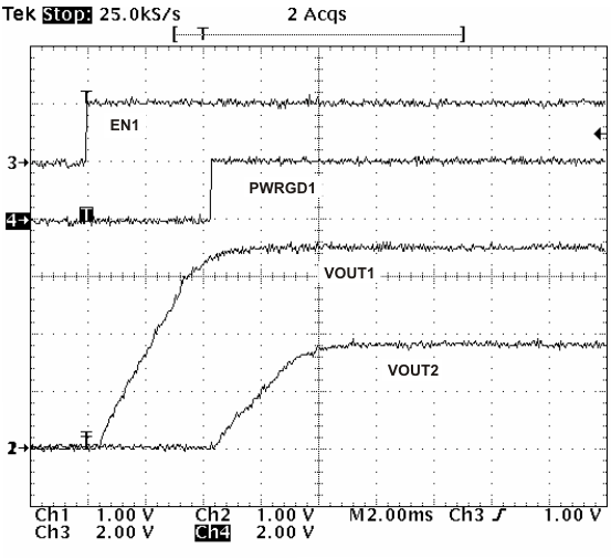 Figure 33. Sequential Startup using EN and PWRGD
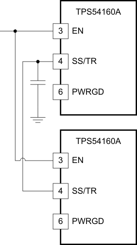 Figure 34. Schematic for Ratiometric Start-Up Using Coupled SS/TR Pins
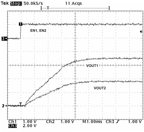 Figure 35. Ratio-Metric Startup using Coupled SS/TR pins
Figure 34 shows a method for ratio-metric start up sequence by connecting the SS/TR pins together. The regulator outputs ramp up to reach regulation at the same time. When calculating the slow start time the pull up current source must be doubled in Equation 6. Figure 35 shows the results of Figure 34.
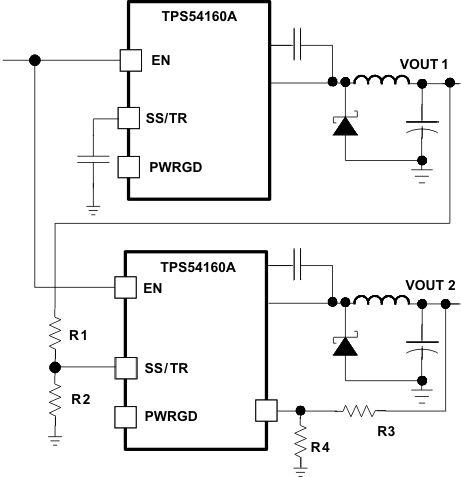 Figure 36. Schematic for Ratiometric and Simultaneous Start-Up Sequence
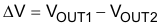
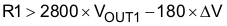
Ratio-metric and simultaneous power supply sequencing can be implemented by connecting the resistor network of R1 and R2 shown in Figure 36 to the output of the power supply that needs to be tracked or another voltage reference source. Using Equation 7 and Equation 8, the tracking resistors can be calculated to initiate the VOUT2 slightly before, after or at the same time as VOUT1. Equation 9 is the voltage difference between VOUT1 and VOUT2 at the 95% of nominal output regulation.
The ΔV variable is zero volts for simultaneous sequencing. To minimize the effect of the inherent SS/TR to VSENSE offset (VSS(offset)) in the slow start circuit and the offset created by the pull-up current source (ISS) and tracking resistors, the VSS(offset) and ISS are included as variables in the equations.
To design a ratio-metric start up in which the VOUT2 voltage is slightly greater than the VOUT1 voltage when VOUT2 reaches regulation, use a negative number in Equation 7 through Equation 9 for ΔV. Equation 9 results in a positive number for applications which the VOUT2 is slightly lower than VOUT1 when VOUT2 regulation is achieved.
Since the SS/TR pin must be pulled below 40 mV before starting after an EN, UVLO or thermal shutdown fault, careful selection of the tracking resistors is needed to ensure the device restarts after a fault. Make sure the calculated R1 value from Equation 7 is greater than the value calculated in Equation 10 to ensure the device can recover from a fault.
As the SS/TR voltage becomes more than 85% of the nominal reference voltage the VSS(offset) becomes larger as the slow start circuits gradually handoff the regulation reference to the internal voltage reference. The SS/TR pin voltage needs to be greater than 1.3 V for a complete handoff to the internal voltage reference as shown in Figure 23.
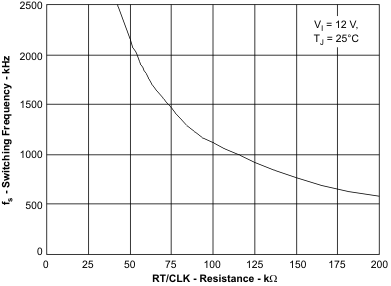
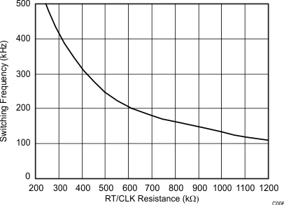
8.3.13 Constant Switching Frequency and Timing Resistor (RT/CLK Pin)
The switching frequency of the TPS54160A is adjustable over a wide range from approximately 100kHz to 2500kHz by placing a resistor on the RT/CLK pin. The RT/CLK pin voltage is typically 0.5V and must have a resistor to ground to set the switching frequency. To determine the timing resistance for a given switching frequency, use Equation 11 or the curves in Figure 40 or Figure 41. To reduce the solution size one would typically set the switching frequency as high as possible, but tradeoffs of the supply efficiency, maximum input voltage and minimum controllable on time should be considered.
The minimum controllable on time is typically 130 ns and limits the maximum operating input voltage.
The maximum switching frequency is also limited by the frequency shift circuit. More discussion on the details of the maximum switching frequency is located below.
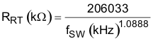
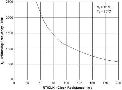 Figure 40. Switching Frequency vs RT/CLK Resistance High Frequency RangeFigure 41. Switching Frequency vs RT/CLK Resistance Low Frequency Range
8.3.14 Overcurrent Protection and Frequency Shift
The TPS54160A implements current mode control which uses the COMP pin voltage to turn off the high-side MOSFET on a cycle by cycle basis. Each cycle the switch current and COMP pin voltage are compared, when the peak switch current intersects the COMP voltage, the high-side switch is turned off. During overcurrent conditions that pull the output voltage low, the error amplifier responds by driving the COMP pin high, increasing the switch current. The error amplifier output is clamped internally, which functions as a switch current limit.
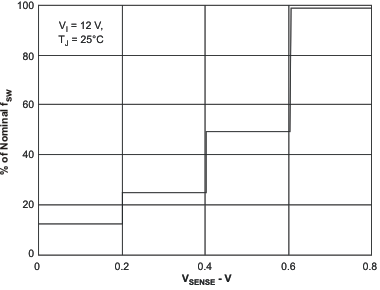
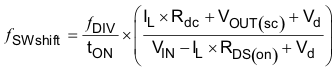
To increase the maximum operating switching frequency at high input voltages the TPS54160A implements a frequency shift. The switching frequency is divided by 8, 4, 2, and 1 as the voltage ramps from 0 to 0.8 volts on VSENSE pin.
The device implements a digital frequency shift to enable synchronizing to an external clock during normal startup and fault conditions. Since the device can only divide the switching frequency by 8, there is a maximum input voltage limit in which the device operates and still have frequency shift protection.
During short-circuit events (particularly with high input voltage applications), the control loop has a finite minimum controllable on time and the output has a low voltage. During the switch on time, the inductor current ramps to the peak current limit because of the high input voltage and minimum on time. During the switch off time, the inductor would normally not have enough off time and output voltage for the inductor to ramp down by the ramp up amount. The frequency shift effectively increases the off time allowing the current to ramp down.
8.3.15 Selecting the Switching Frequency
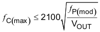
The switching frequency that is selected should be the lower value of the two equations, Equation 12 and Equation 13. Equation 12 is the maximum switching frequency limitation set by the minimum controllable on time. Setting the switching frequency above this value causes the regulator to skip switching pulses.
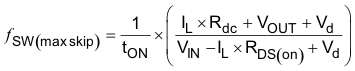
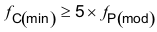
Equation 13 is the maximum switching frequency limit set by the frequency shift protection. To have adequate output short circuit protection at high input voltages, the switching frequency should be set to be less than the fSW(maxshift) frequency. In Equation 13, to calculate the maximum switching frequency, consider that the output voltage decreases from the nominal voltage to 0 V, the fDIV integer increases from 1 to 8 corresponding to the frequency shift.
In Figure 42, the solid line illustrates a typical safe operating area regarding frequency shift and assumes the output voltage is 0 V, and the resistance of the inductor is 0.1Ω, FET on-resistance of 0.2 Ω and the diode voltage drop is 0.5 V. The dashed line is the maximum switching frequency to avoid pulse skipping. Enter these equations in a spreadsheet or other software or use the SwitcherPro design software to determine the switching frequency.
| IL | inductor current |
| Rdc | inductor resistance |
| VIN | maximum input voltage |
| VOUT | output voltage |
| VOUT(sc) | output voltage during short |
| Vd | diode voltage drop |
| RDS(on) | switch on resistance |
| tON | controllable on time |
| ƒDIV | frequency divide equals (1, 2, 4, or 8) |
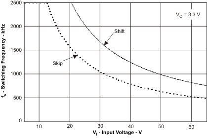 Figure 42. Maximum Switching Frequency vs. Input Voltage
8.3.16 How to Interface to RT/CLK Pin
The RT/CLK pin can be used to synchronize the regulator to an external system clock. To implement the synchronization feature connect a square wave to the RT/CLK pin through the circuit network shown in Figure 43. The square wave amplitude must transition lower than 0.5V and higher than 2.2V on the RT/CLK pin and have an on time greater than 40 ns and an off time greater than 40 ns. The synchronization frequency range is 300 kHz to 2200 kHz. The rising edge of the PH is synchronized to the falling edge of RT/CLK pin signal. The external synchronization circuit should be designed in such a way that the device has the default frequency set resistor connected from the RT/CLK pin to ground should the synchronization signal turn off. It is recommended to use a frequency set resistor connected as shown in Figure 43 through a 50Ω resistor to ground. The resistor should set the switching frequency close to the external CLK frequency. It is recommended to ac couple the synchronization signal through a 10 pF ceramic capacitor to RT/CLK pin and a 4kΩ series resistor. The series resistor reduces PH jitter in heavy load applications when synchronizing to an external clock and in applications which transition from synchronizing to RT mode. The first time the CLK is pulled above the CLK threshold the device switches from the RT resistor frequency to PLL mode. The internal 0.5V voltage source is removed and the CLK pin becomes high impedance as the PLL starts to lock onto the external signal. Since there is a PLL on the regulator the switching frequency can be higher or lower than the frequency set with the external resistor. The device transitions from the resistor mode to the PLL mode and then will increase or decrease the switching frequency until the PLL locks onto the CLK frequency within 100 microseconds.
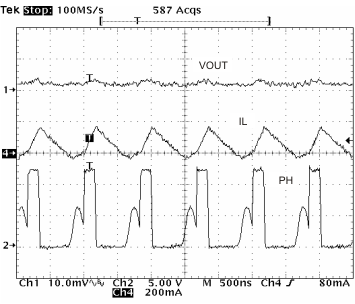
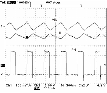
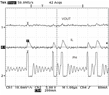
When the device transitions from the PLL to resistor mode the switching frequency will slow down from the CLK frequency to 150 kHz, then reapply the 0.5V voltage and the resistor will then set the switching frequency. The switching frequency is divided by 8, 4, 2, and 1 as the voltage ramps from 0 to 0.8 volts on VSENSE pin. The device implements a digital frequency shift to enable synchronizing to an external clock during normal startup and fault conditions. Figure 44, Figure 45 and Figure 46 show the device synchronized to an external system clock in continuous conduction mode (ccm) discontinuous conduction (dcm) and pulse skip mode (psm).
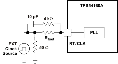 Figure 43. Synchronizing to a System Clock
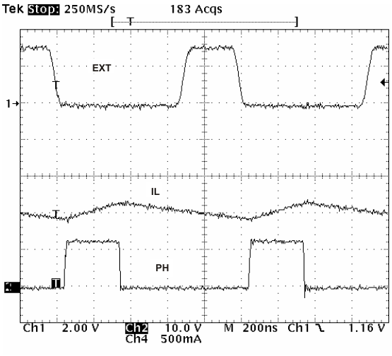 Figure 44. Plot of Synchronizing in CCM
 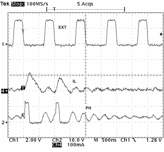 Figure 46. Plot of Synchronizing in PSM
 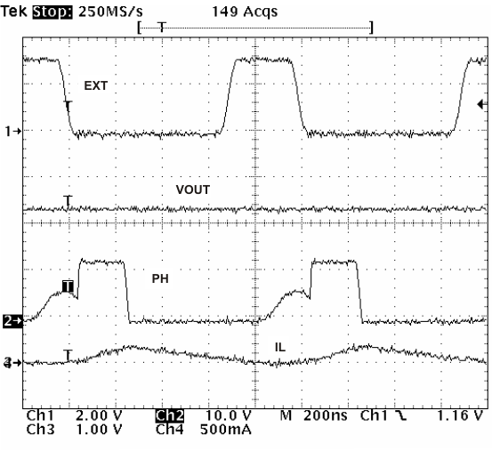 Figure 45. Plot of Synchronizing in DCM
 8.3.17 Power Good (PWRGD Pin)
The PWRGD pin is an open drain output. Once the VSENSE pin is between 94% and 107% of the internal voltage reference the PWRGD pin is de-asserted and the pin floats. It is recommended to use a pull-up resistor between the values of 10 and 100kΩ to a voltage source that is 5.5V or less. The PWRGD is in a defined state once the VIN input voltage is greater than 1.5V but with reduced current sinking capability. The PWRGD will achieve full current sinking capability as VIN input voltage approaches 3V.
The PWRGD pin is pulled low when the VSENSE is lower than 92% or greater than 109% of the nominal internal reference voltage. Also, the PWRGD is pulled low, if the UVLO or thermal shutdown are asserted or the EN pin pulled low.
8.3.18 Overvoltage Transient Protection
The TPS54160A incorporates an overvoltage transient protection (OVTP) circuit to minimize voltage overshoot when recovering from output fault conditions or strong unload transients on power supply designs with low value output capacitance. For example, when the power supply output is overloaded the error amplifier compares the actual output voltage to the internal reference voltage. If the VSENSE pin voltage is lower than the internal reference voltage for a considerable time, the output of the error amplifier will respond by clamping the error amplifier output to a high voltage. Thus, requesting the maximum output current. Once the condition is removed, the regulator output rises and the error amplifier output transitions to the steady state duty cycle. In some applications, the power supply output voltage can respond faster than the error amplifier output can respond, this actuality leads to the possibility of an output overshoot. The OVTP feature minimizes the output overshoot, when using a low value output capacitor, by implementing a circuit to compare the VSENSE pin voltage to OVTP threshold which is 109% of the internal voltage reference. If the VSENSE pin voltage is greater than the OVTP threshold, the high-side MOSFET is disabled preventing current from flowing to the output and minimizing output overshoot. When the VSENSE voltage drops lower than the OVTP threshold, the high-side MOSFET is allowed to turn on at the next clock cycle.
8.3.19 Thermal Shutdown
The device implements an internal thermal shutdown to protect itself if the junction temperature exceeds 182°C. The thermal shutdown forces the device to stop switching when the junction temperature exceeds the thermal trip threshold. Once the die temperature decreases below 182°C, the device reinitiates the power up sequence by discharging the SS/TR pin.
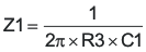
8.3.20 Small Signal Model for Loop Response
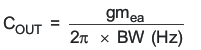
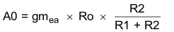
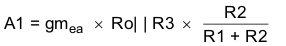
Figure 47 shows an equivalent model for the TPS54160A control loop which can be modeled in a circuit simulation program to check frequency response and dynamic load response. The error amplifier is a transconductance amplifier with a gmEA of 97 μA/V. The error amplifier can be modeled using an ideal voltage controlled current source. The resistor RO and capacitor CO model the open loop gain and frequency response of the amplifier. The 1mV ac voltage source between the nodes a and b effectively breaks the control loop for the frequency response measurements. Plotting c/a shows the small signal response of the frequency compensation. Plotting a/b shows the small signal response of the overall loop. The dynamic loop response can be checked by replacing RL with a current source with the appropriate load step amplitude and step rate in a time domain analysis. This equivalent model is only valid for continuous conduction mode designs.
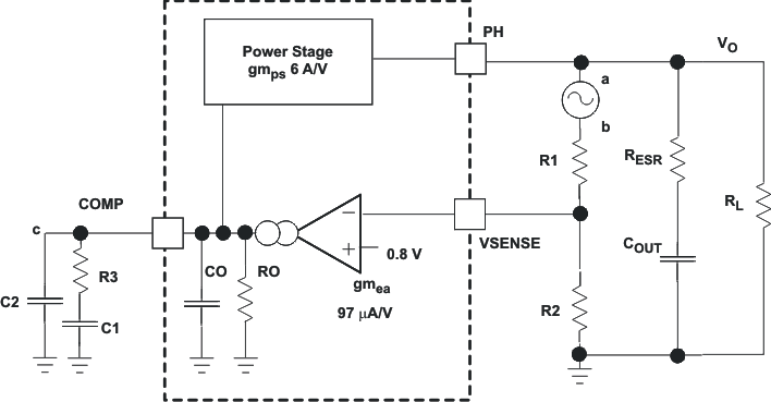 Figure 47. Small Signal Model for Loop Response
8.3.21 Simple Small Signal Model for Peak Current Mode Control
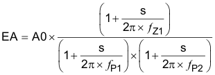
Figure 48 describes a simple small signal model that can be used to understand how to design the frequency compensation. The TPS54160A power stage can be approximated to a voltage-controlled current source (duty cycle modulator) supplying current to the output capacitor and load resistor. The control to output transfer function is shown in Equation 14 and consists of a dc gain, one dominant pole, and one ESR zero. The quotient of the change in switch current and the change in COMP pin voltage (node c in Figure 47) is the power stage transconductance. The gmPS for the TPS54160A is 6 A/V. The low-frequency gain of the power stage frequency response is the product of the transconductance and the load resistance as shown in Equation 15.
As the load current increases and decreases, the low-frequency gain decreases and increases, respectively. This variation with the load may seem problematic at first glance, but fortunately the dominant pole moves with the load current (see Equation 16). The combined effect is highlighted by the dashed line in the right half of Figure 48. As the load current decreases, the gain increases and the pole frequency lowers, keeping the 0-dB crossover frequency the same for the varying load conditions which makes it easier to design the frequency compensation. The type of output capacitor chosen determines whether the ESR zero has a profound effect on the frequency compensation design. Using high ESR aluminum electrolytic capacitors may reduce the number frequency compensation components needed to stabilize the overall loop because the phase margin increases from the ESR zero at the lower frequencies (see Equation 17).
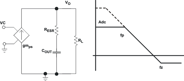 Figure 48. Simple Small Signal Model and Frequency Response for Peak Current Mode Control

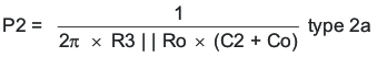
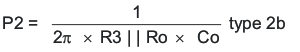
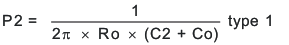
8.3.22 Small Signal Model for Frequency Compensation
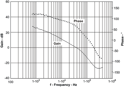
The TPS54160A uses a transconductance amplifier for the error amplifier and readily supports three of the commonly-used frequency compensation circuits. Compensation circuits Type 2A, Type 2B, and Type 1 are shown in Figure 49. Type 2 circuits most likely implemented in high bandwidth power-supply designs using low ESR output capacitors. The Type 1 circuit is used with power-supply designs with high-ESR aluminum electrolytic or tantalum capacitors.. Equation 18 and Equation 19 show how to relate the frequency response of the amplifier to the small signal model in Figure 49. The open-loop gain and bandwidth are modeled using the RO and CO shown in Figure 49. See the application section for a design example using a Type 2A network with a low ESR output capacitor.
Equation 18 through Equation 27 are provided as a reference for those who prefer to compensate using the preferred methods. Those who prefer to use prescribed method use the method outlined in the application section or use switched information.
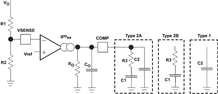 Figure 49. Types of Frequency Compensation
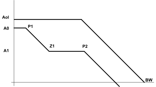 Figure 50. Frequency Response of the Type 2A and Type 2B Frequency Compensation
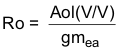
8.4 Device Functional Modes
8.4.1 Operation with VIN < 3.5 V (Minimum VIN)
The device is recommended to operate with input voltages above 3.5 V. The typical VIN UVLO threshold is 2.5 V and the device may operate at input voltages down to the UVLO voltage. At input voltages below the actual UVLO voltage, the device will not switch. The PWRGD output will be controlled once VIN is above 1.5 V maximum. If EN is externally pulled up to VIN or left floating, when VIN passes the UVLO threshold the device will become active. Switching is enabled the soft start sequence is initiated. The TPS54160 will start at the soft start time determined by the external soft start capacitor at the SS/TR pin.
8.4.2 Operation with EN Control
The enable threshold voltage is 1.25 V typical. With EN held below that voltage the device is disabled and switching is inhibited even if VIN is above its UVLO threshold. The IC quiescent current is reduced in this state. If the EN voltage is increased above the threshold while VIN is above its UVLO threshold, the device becomes active. Switching is enabled, and the soft start sequence is initiated. The TPS54160 will start at the soft start time determined by the external slow start capacitor at the SS/TR pin.
9 Application and Implementation
9.1 Application Information
TPS5426x devices are part of a family of non-synchronous, step-down converters with an integrated high-side FET and 100% duty cycle capability. Idea applications are 12-V, 24-V and 48-V industrial and commercial low power systems. Aftermarket Auto Accessories: Video, GPS, Entertainment
9.2 Typical Application
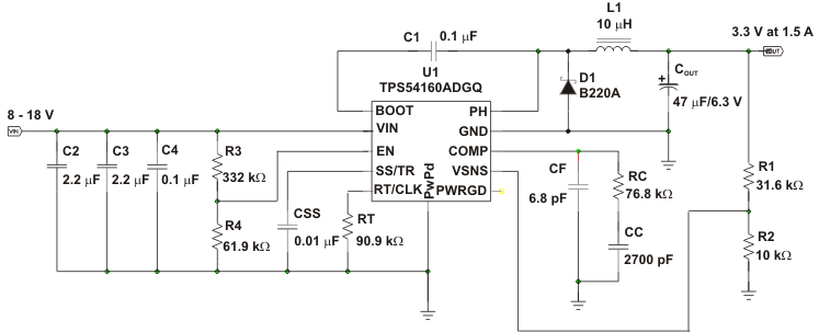 Figure 51. High Frequency, 3.3V Output Power Supply Design with Adjusted UVLO.
 9.2.1 Design Requirements
This example details the design of a high frequency switching regulator design using ceramic output capacitors. A few parameters must be known in order to start the design process. These parameters are typically determined at the system level. For this example, we will start with the following known parameters:
Table 1. Design Parameters
9.2.2 Detailed Design Procedures
9.2.2.1 Selecting the Switching Frequency
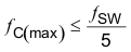
The first step is to decide on a switching frequency for the regulator. Typically, the user will want to choose the highest switching frequency possible since this will produce the smallest solution size. The high switching frequency allows for lower valued inductors and smaller output capacitors compared to a power supply that switches at a lower frequency. The switching frequency that can be selected is limited by the minimum on-time of the internal power switch, the input voltage and the output voltage and the frequency shift limitation.
Equation 12 and Equation 13 must be used to find the maximum switching frequency for the regulator, choose the lower value of the two equations. Switching frequencies higher than these values will result in pulse skipping or the lack of overcurrent protection during a short circuit.
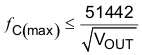
The typical minimum on time, tonmin, is 130 ns for the TPS54160A. For this example, the output voltage is 3.3 V and the maximum input voltage is 18 V, which allows for a maximum switch frequency up to 1600 kHz when including the inductor resistance, on resistance and diode voltage in Equation 12. To ensure overcurrent runaway is not a concern during short circuits in your design use Equation 13 or the solid curve in Figure 42 to determine the maximum switching frequency. With a maximum input voltage of 20 V, for some margin above 18 V, assuming a diode voltage of 0.5 V, inductor resistance of 100 mΩ, switch resistance of 200mΩ, a current limit value of 2.7 A, the maximum switching frequency is approximately 2500kHz.
Choosing the lower of the two values and adding some margin a switching frequency of 1200 kHz is used. To determine the timing resistance for a given switching frequency, use Equation 11 or the curve in Figure 40.
The switching frequency is set by resistor Rt shown in Figure 51.
9.2.2.2 Output Inductor Selection (LO)
To calculate the minimum value of the output inductor, use Equation 28.
KIND is a coefficient that represents the amount of inductor ripple current relative to the maximum output current.
The inductor ripple current will be filtered by the output capacitor. Therefore, choosing high inductor ripple currents will impact the selection of the output capacitor since the output capacitor must have a ripple current rating equal to or greater than the inductor ripple current. In general, the inductor ripple value is at the discretion of the designer; however, the following guidelines may be used.
For designs using low ESR output capacitors such as ceramics, a value as high as KIND = 0.3 may be used. When using higher ESR output capacitors, KIND = 0.2 yields better results. Since the inductor ripple current is part of the PWM control system, the inductor ripple current should always be greater than 100 mA for dependable operation. In a wide input voltage regulator, it is best to choose an inductor ripple current on the larger side. This allows the inductor to still have a measurable ripple current with the input voltage at its minimum.
For this design example, use KIND = 0.2 and the minimum inductor value is calculated to be 7.6μH. For this design, a nearest standard value was chosen: 10μH. For the output filter inductor, it is important that the RMS current and saturation current ratings not be exceeded. The RMS and peak inductor current can be found from Equation 30 and Equation 31.
For this design, the RMS inductor current is 1.506 A and the peak inductor current is 1.62 A. The chosen inductor is a MSS6132-103. It has a saturation current rating of 1.64 A and an RMS current rating of 1.9A.
As the equation set demonstrates, lower ripple currents will reduce the output voltage ripple of the regulator but will require a larger value of inductance. Selecting higher ripple currents will increase the output voltage ripple of the regulator but allow for a lower inductance value.
The current flowing through the inductor is the inductor ripple current plus the output current. During power up, faults or transient load conditions, the inductor current can increase above the calculated peak inductor current level calculated above. In transient conditions, the inductor current can increase up to the switch current limit of the device. For this reason, the most conservative approach is to specify an inductor with a saturation current rating equal to or greater than the switch current limit rather than the peak inductor current.
9.2.2.3 Output Capacitor
There are three primary considerations for selecting the value of the output capacitor. The output capacitor will determine the modulator pole, the output voltage ripple, and how the regulators responds to a large change in load current. The output capacitance needs to be selected based on the more stringent of these three criteria.
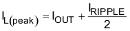
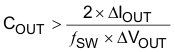
The desired response to a large change in the load current is the first criteria. The output capacitor needs to supply the load with current when the regulator can not. This situation would occur if there are desired hold-up times for the regulator where the output capacitor must hold the output voltage above a certain level for a specified amount of time after the input power is removed. The regulator also will temporarily not be able to supply sufficient output current if there is a large, fast increase in the current needs of the load such as transitioning from no load to a full load. The regulator usually needs two or more clock cycles for the control loop to see the change in load current and output voltage and adjust the duty cycle to react to the change. The output capacitor must be sized to supply the extra current to the load until the control loop responds to the load change. The output capacitance must be large enough to supply the difference in current for twoclock cycles while only allowing a tolerable amount of droop in the output voltage. Equation 32 shows the minimum output capacitance necessary to accomplish this.
Where ΔIOUT is the change in output current, ƒsw is the regulators switching frequency and ΔVout is the allowable change in the output voltage. For this example, the transient load response is specified as a 4% change in VOUT for a load step from 0 A (no load) to 1.5 A (full load). For this example, ΔIOUT = 1.5-0 = 1.5 A and ΔVOUT = 0.04 × 3.3 = 0.132 V. Using these numbers gives a minimum capacitance of 18.9 μF. This value does not take the ESR of the output capacitor into account in the output voltage change. For ceramic capacitors, the ESR is usually small enough to ignore in this calculation. Aluminum electrolytic and tantalum capacitors have higher ESR that should be taken into account.
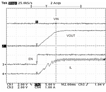
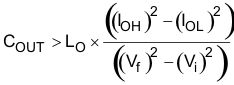
The catch diode of the regulator cannot sink current so any stored energy in the inductor produces an output voltage overshoot when the load current rapidly decreases, see Figure 52. The output capacitor must also be sized to absorb energy stored in the inductor when transitioning from a high load current to a lower load current. The excess energy that gets stored in the output capacitor increases the voltage on the capacitor. The capacitor must be sized to maintain the desired output voltage during these transient periods. Equation 33 is used to calculate the minimum capacitance to keep the output voltage overshoot to a desired value. Where L is the value of the inductor, IOH is the output current under heavy load, IOL is the output under light load, Vf is the final peak output voltage, and Vi is the initial capacitor voltage. For this example, the worst case load step will be from 1.5 A to 0 A. The output voltage increases during this load transition and the stated maximum in our specification is 4% of the output voltage. This will make Vf = 1.04 × 3.3 = 3.432. Vi is the initial capacitor voltage which is the nominal output voltage of 3.3 V. Using these numbers in Equation 33 yields a minimum capacitance of 25.3 μF.
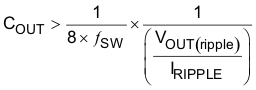
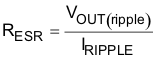
Equation 34 calculates the minimum output capacitance needed to meet the output voltage ripple specification. Where fSW is the switching frequency, VOUT(ripple) is the maximum allowable output voltage ripple, and Iripple is the inductor ripple current. Equation 34 yields 0.7 μF.
Equation 35 calculates the maximum ESR an output capacitor can have to meet the output voltage ripple specification. Equation 35 indicates the ESR should be less than 147 mΩ.
The most stringent criteria for the output capacitor is 25.3 μF of capacitance to keep the output voltage in regulation during an unload transient.
Additional capacitance de-ratings for aging, temperature and dc bias should be factored in which increases this minimum value. For this example, a 47 μF 6.3V X7R ceramic capacitor with 5 mΩ of ESR is used.
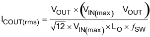
Capacitors generally have limits to the amount of ripple current they can handle without failing or producing excess heat. An output capacitor that can support the inductor ripple current must be specified. Some capacitor data sheets specify the Root Mean Square (RMS) value of the maximum ripple current. Equation 36 can be used to calculate the RMS ripple current the output capacitor needs to support. For this application, Equation 36 yields 64.8 mA.
9.2.2.4 Catch Diode
The TPS54160A requires an external catch diode between the PH pin and GND. The selected diode must have a reverse voltage rating equal to or greater than Vinmax. The peak current rating of the diode must be greater than the maximum inductor current. The diode should also have a low forward voltage. Schottky diodes are typically a good choice for the catch diode due to their low forward voltage. The lower the forward voltage of the diode, the higher the efficiency of the regulator.
Typically, the higher the voltage and current ratings the diode has, the higher the forward voltage will be. Since the design example has an input voltage up to 18 V, a diode with a minimum of 20V reverse voltage will be selected.
For the example design, the B220A Schottky diode is selected for its lower forward voltage and it comes in a larger package size which has good thermal characteristics over small devices. The typical forward voltage of the B220A is 0.50 V.
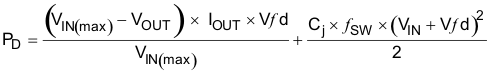
The diode must also be selected with an appropriate power rating. The diode conducts the output current during the off-time of the internal power switch. The off-time of the internal switch is a function of the maximum input voltage, the output voltage, and the switching frequency. The output current during the off-time is multiplied by the forward voltage of the diode which equals the conduction losses of the diode. At higher switch frequencies, the ac losses of the diode need to be taken into account. The ac losses of the diode are due to the charging and discharging of the junction capacitance and reverse recovery. Equation 37 is used to calculate the total power dissipation, conduction losses plus ac losses, of the diode.
The B220A has a junction capacitance of 120pF. Using Equation 37, the selected diode will dissipate 0.632 W. This power dissipation, depending on mounting techniques, should produce a 16°C temperature rise in the diode when the input voltage is 18 V and the load current is 1.5 A.
If the power supply spends a significant amount of time at light load currents or in sleep mode consider using a diode which has a low leakage current and slightly higher forward voltage drop.
9.2.2.5 Input Capacitor
The TPS54160A requires a high quality ceramic, type X5R or X7R, input decoupling capacitor of at least 3 μF of effective capacitance and in some applications a bulk capacitance. The effective capacitance includes any dc bias effects. The voltage rating of the input capacitor must be greater than the maximum input voltage. The capacitor must also have a ripple current rating greater than the maximum input current ripple of the TPS54160A. The input ripple current can be calculated using Equation 38.
The value of a ceramic capacitor varies significantly over temperature and the amount of dc bias applied to the capacitor. The capacitance variations due to temperature can be minimized by selecting a dielectric material that is stable over temperature. X5R and X7R ceramic dielectrics are usually selected for power regulator capacitors because they have a high capacitance to volume ratio and are fairly stable over temperature. The output capacitor must also be selected with the dc bias taken into account. The capacitance value of a capacitor decreases as the dc bias across a capacitor increases.
For this example design, a ceramic capacitor with at least a 20 V voltage rating is required to support the maximum input voltage. Common standard ceramic capacitor voltage ratings include 4 V, 6.3 V, 10 V, 16 V, 25 V, 50 V or 100 V, so a 25 V capacitor should be selected. For this example, two 2.2 μF, 25 V capacitors in parallel have been selected. Table 2 shows a selection of high voltage capacitors. The input capacitance value determines the input ripple voltage of the regulator. The input voltage ripple can be calculated using Equation 39. Using the design example values
- IOUT(max) = 1.5 A
- CIN = 4.4 μF
- ƒSW = 1200 kHz
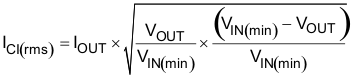
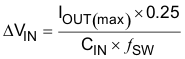
Table 2. Capacitor Types
| VALUE (μF) | EIA Size | VOLTAGE (V) | DIALECTRIC | COMMENTS |
|---|---|---|---|---|
| 1.0 to 2.2 | 1210 | 100 | X7R | GRM32 series |
| 1.0 to 4.7 | 50 | |||
| 1.0 | 1206 | 100 | GRM31 series | |
| 1.0 to 2.2 | 50 | |||
| 1.0 10 1.8 | 2220 | 50 | VJ X7R series | |
| 1.0 to 1.2 | 100 | |||
| 1.0 to 3.9 | 2225 | 50 | ||
| 1.0 to 1.8 | 100 | |||
| 1.0 to 2.2 | 1812 | 100 | C series C4532 | |
| 1.5 to 6.8 | 50 | |||
| 1.0. to 2.2 | 1210 | 100 | C series C3225 | |
| 1.0 to 3.3 | 50 | |||
| 1.0 to 4.7 | 1210 | 50 | X7R dielectric series | |
| 1.0 | 100 | |||
| 1.0 to 4.7 | 1812 | 50 | ||
| 1.0 to 2.2 | 100 |
9.2.2.6 Slow Start Capacitor
The slow start capacitor determines the minimum amount of time it will take for the output voltage to reach its nominal programmed value during power up. This is useful if a load requires a controlled voltage slew rate. This is also used if the output capacitance is large and would require large amounts of current to quickly charge the capacitor to the output voltage level. The large currents necessary to charge the capacitor may make the TPS54160A reach the current limit or excessive current draw from the input power supply may cause the input voltage rail to sag. Limiting the output voltage slew rate solves both of these problems.
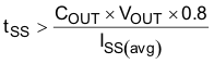
The slow start time must be long enough to allow the regulator to charge the output capacitor up to the output voltage without drawing excessive current. Equation 40 can be used to find the minimum slow start time, tss, necessary to charge the output capacitor, Cout, from 10% to 90% of the output voltage, Vout, with an average slow start current of Issavg. In the example, to charge the 47μF output capacitor up to 3.3V while only allowing the average input current to be 0.125A would require a 1 ms slow start time.
Once the slow start time is known, the slow start capacitor value can be calculated using Equation 6. For the example circuit, the slow start time is not too critical since the output capacitor value is 47μF which does not require much current to charge to 3.3V. The example circuit has the slow start time set to an arbitrary value of 1ms which requires a 3.3 nF capacitor.
9.2.2.7 Bootstrap Capacitor Selection
A 0.1-μF ceramic capacitor must be connected between the BOOT and PH pins for proper operation. It is recommended to use a ceramic capacitor with X5R or better grade dielectric. The capacitor should have a 10V or higher voltage rating.
9.2.2.8 Under Voltage Lock Out Set Point
The Under Voltage Lock Out (UVLO) can be adjusted using an external voltage divider on the EN pin of the TPS54160A. The UVLO has two thresholds, one for power up when the input voltage is rising and one for power down or brown outs when the input voltage is falling. For the example design, the supply should turn on and start switching once the input voltage increases above 7.7V (enabled). After the regulator starts switching, it should continue to do so until the input voltage falls below 6.7V (UVLO stop).
The programmable UVLO and enable voltages are set using a resistor divider between VIN and ground to the EN pin. Equation 2 through Equation 3 can be used to calculate the resistance values necessary. For the example application, a 332kΩ between VIN and EN and a 61.9kΩ between EN and ground are required to produce the 7.7 and 6.7 volt start and stop voltages.
9.2.2.9 Output Voltage and Feedback Resistors Selection
For the example design, 10.0 kΩ was selected for R2. Using Equation 1, R1 is calculated as 31.25 kΩ. The nearest standard 1% resistor is 31.6 kΩ. Due to current leakage of the VSENSE pin, the current flowing through the feedback network should be greater than 1 μA in order to maintain the output voltage accuracy. This requirement makes the maximum value of R2 equal to 800 kΩ. Choosing higher resistor values will decrease quiescent current and improve efficiency at low output currents but may introduce noise immunity problems.
9.2.2.10 Compensation
There are several industry techniques used to compensate DC/DC regulators. The method presented here yields high phase margins. For most conditions, the regulator will have a phase margin between 60 and 90 degrees. The method presented here ignores the effects of the slope compensation that is internal to the TPS54160A. Since the slope compensation is ignored, the actual crossover frequency is usually lower than the crossover frequency used in the calculations.
Use SwitcherPro software for a more accurate design.
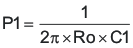
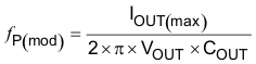
The uncompensated regulator will have a dominant pole, typically located between 300 Hz and 3 kHz, due to the output capacitor and load resistance and a pole due to the error amplifier. One zero exists due to the output capacitor and the ESR. The zero frequency is higher than either of the two poles.
If left uncompensated, the double pole created by the error amplifier and the modulator would lead to an unstable regulator. To stabilize the regulator, one pole must be canceled out. One design approach is to locate a compensating zero at the modulator pole. Then select a crossover frequency that is higher than the modulator pole. The gain of the error amplifier can be calculated to achieve the desired crossover frequency. The capacitor used to create the compensation zero along with the output impedance of the error amplifier form a low frequency pole to provide a minus one slope through the crossover frequency. Then a compensating pole is added to cancel the zero due to the output capacitors ESR. If the ESR zero resides at a frequency higher than the switching frequency then it can be ignored.
To compensate the TPS54160A using this method, first calculate the modulator pole and zero using the following equations:
where
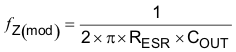
For the example design, the modulator pole is located at 1.5 kHz and the ESR zero is located at 338 kHz.
Next, the designer selects a crossover frequency which will determine the bandwidth of the control loop. The crossover frequency must be located at a frequency at least five times higher than the modulator pole. The crossover frequency must also be selected so that the available gain of the error amplifier at the crossover frequency is high enough to allow for proper compensation.
Equation 47 is used to calculate the maximum crossover frequency when the ESR zero is located at a frequency that is higher than the desired crossover frequency. This will usually be the case for ceramic or low ESR tantalum capacitors. Aluminum Electrolytic and Tantalum capacitors will typically produce a modulator zero at a low frequency due to their high ESR.
The example application is using a low ESR ceramic capacitor with 10mΩ of ESR making the zero at 338 kHz.
This value is much higher than typical crossover frequencies so the maximum crossover frequency is calculated using both Equation 43 and Equation 46.
Using Equation 46 gives a minimum crossover frequency of 7.6 kHz and Equation 43 gives a maximum crossover frequency of 45.3 kHz.
A crossover frequency of 45 kHz is arbitrarily selected from this range.
For ceramic capacitors use Equation 43:
For tantalum or aluminum capacitors use Equation 44:
For all cases use Equation 45 and Equation 46:
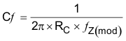
Once a crossover frequency, ƒC, has been selected, the gain of the modulator at the crossover frequency is calculated. The gain of the modulator at the crossover frequency is calculated using Equation 47 .
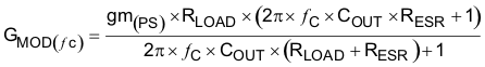
For the example problem, the gain of the modulator at the crossover frequency is 0.542. Next, the compensation components are calculated. A resistor in series with a capacitor is used to create a compensating zero. A capacitor in parallel to these two components forms the compensating pole. However, calculating the values of these components varies depending on if the ESR zero is located above or below the crossover frequency. For ceramic or low ESR tantalum output capacitors, the zero will usually be located above the crossover frequency. For aluminum electrolytic and tantalum capacitors, the modulator zero is usually located lower in frequency than the crossover frequency. For cases where the modulator zero is higher than the crossover frequency (ceramic capacitors).
For cases where the modulator zero is less than the crossover frequency (Aluminum or Tantalum capacitors), the equations are:
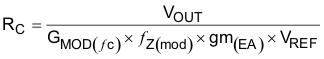
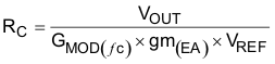
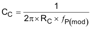
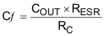
For the example problem, the ESR zero is located at a higher frequency compared to the crossover frequency so Equation 50 through Equation 53 are used to calculate the compensation components. In this example, the calculated components values are:
- RC = 76.2 kΩ
- CC = 2710 pF
- Cƒ = 6.17 pF
The calculated value of the Cf capacitor is not a standard value so a value of 2700 pF is used. 6.8 pF is used for CC. The RC resistor sets the gain of the error amplifier which determines the crossover frequency. The calculated RC resistor is not a standard value, so 76.8 kΩ is used.
9.2.2.11 Power Dissipation Estimate
The following formulas show how to estimate the device power dissipation under continuous conduction mode (CCM) operation. These equations should not be used if the device is working in discontinuous conduction mode (DCM).
The power dissipation of the device includes conduction loss (Pcon), switching loss (Psw), gate drive loss (Pgd) and supply current (Pq).
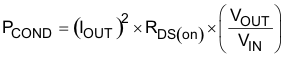
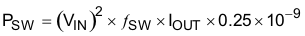
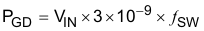
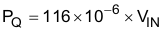
where

For given TA,
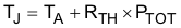
For given TJMAX = 150°C
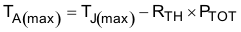
where
There are additional power losses in the regulator circuit due to the inductor ac and dc losses, the catch diode and trace resistance that will impact the overall efficiency of the regulator.
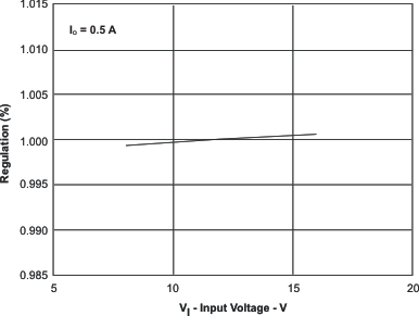
9.2.3 Application Curves